TLI4946
List of Figures
List of Figures
Figure 1
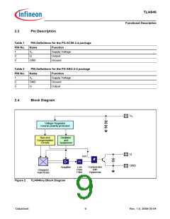
Figure 2
Figure 3
Figure 4
Figure 5
Figure 6
Figure 7
Figure 8
Figure 9
Pin Configuration and sensitive area (Top view, figure not to scale) . . . . . . . . . . . . . . . . . . . . . . . . 8
TLI4946xy Block Diagram. . . . . . . . . . . . . . . . . . . . . . . . . . . . . . . . . . . . . . . . . . . . . . . . . . . . . . . . . 9
Definition of the Magnetic Field direction . . . . . . . . . . . . . . . . . . . . . . . . . . . . . . . . . . . . . . . . . . . . 10
Output Signal . . . . . . . . . . . . . . . . . . . . . . . . . . . . . . . . . . . . . . . . . . . . . . . . . . . . . . . . . . . . . . . . . 10
Application circuit . . . . . . . . . . . . . . . . . . . . . . . . . . . . . . . . . . . . . . . . . . . . . . . . . . . . . . . . . . . . . . 11
Timing Diagram . . . . . . . . . . . . . . . . . . . . . . . . . . . . . . . . . . . . . . . . . . . . . . . . . . . . . . . . . . . . . . . 13
Marking of the TLI4946K and TLI4946-2K distance of the chip to the upper side . . . . . . . . . . . . . 14
PG-SC59-3-4 Package Outline. . . . . . . . . . . . . . . . . . . . . . . . . . . . . . . . . . . . . . . . . . . . . . . . . . . . 14
Footprint PG-SC59-3-4 (SOT23 compatible) . . . . . . . . . . . . . . . . . . . . . . . . . . . . . . . . . . . . . . . . . 15
Figure 10 Marking of the TLI4946-2L and distance of the chip to the upper side. . . . . . . . . . . . . . . . . . . . . . 15
Figure 11 PG-SSO-3-2 Package Outline . . . . . . . . . . . . . . . . . . . . . . . . . . . . . . . . . . . . . . . . . . . . . . . . . . . . 16
Datasheet
5
Rev. 1.0, 2009-05-04

 INFINEON [ Infineon ]