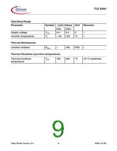
TLE 6250
TLE 6250 V33
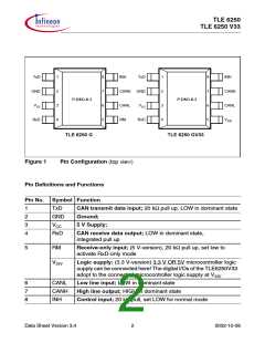
TxD
GND
VCC
1
2
3
4
8
7
6
5
INH
TxD
1
2
3
4
8
7
6
5
INH
CANH GND
CANH
CANL
V33V
P-DSO-8-3
P-DSO-8-3
CANL
RM
VCC
RxD
RxD
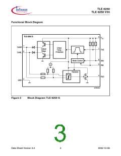
TLE 6250 G
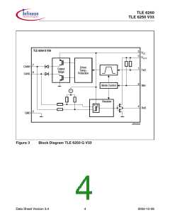
TLE 6250 GV33
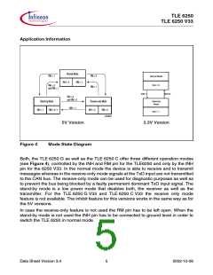
Figure 1
Pin Configuration (top view)
Pin Definitions and Functions
Pin No. Symbol Function
1
2
3
4
TxD
GND
VCC
CAN transmit data input; 20 kΩ pull up, LOW in dominant state
Ground;
5 V Supply;
RxD
CAN receive data output; LOW in dominant state,
integrated pull up
5
RM
Receive-only input; (5 V-version), 20 kΩ pull up, set low to
activate RxD-only mode
V33V
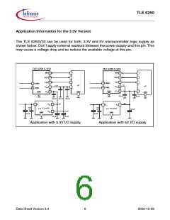
Logic supply; (3.3 V-version) 3.3 V OR 5V microcontroller logic
supply can be connected here! The digital I/Os of the TLE6250V33
adopt to the connected microcontroller logic supply at V33V
6
7
8
CANL
CANH
INH
Low line input; LOW in dominant state
High line output; HIGH in dominant state
Control input; 20 kΩ pull, set LOW for normal mode
Data Sheet Version 3.4
2
2002-10-08

 INFINEON [ Infineon ]