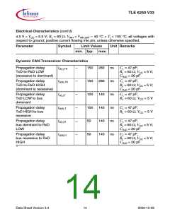
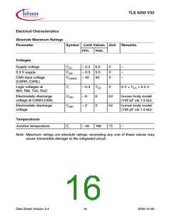
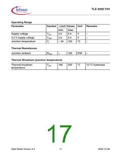
TLE 6250 V33
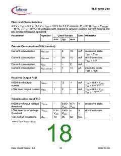
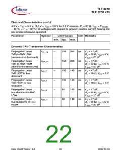
Electrical Characteristics
4.5 V < VCC < 5.5 V; (3.0 V < V33V < 3.6 V for 3.3 V version); RL = 60 Ω; VINH < VINH,ON
;
– 40 °C < Tj < 150 °C; all voltages with respect to ground; positive current flowing into
pin; unless otherwise specified.
Parameter
Symbol
Limit Values
Unit Remarks
min. typ. max.
Current Consumption (3.3V version)
Current consumption
Current consumption
ICC+33V
ICC+33V
–
–
6
10
70
mA recessive state;
V
TxD = V33V
mA dominant state;
TxD = 0 V
45
V
Current consumption
Current consumption
I33V
–
–
–
2
mA
ICC+33V,stb
1
10
µA stand-by mode
TxD = high
Receiver Output R×D
HIGH level output
current
IRD,H
–
-2
2
-1
mA VRD = 0.8 × V33V,
Vdiff < 0.4 Vnote 1)
LOW level output current IRD,L
1
–
mA VRD = 0.2 × V33V,
Vdiff > 1 Vnote 1)
Transmission Input T×D
HIGH level input voltage VTD,H
threshold
–
0.55× 0.7×
V
recessive state;
dominant state;
–
V33V V33V
LOW level input voltage VTD,L
threshold
0.3× 0.45× –
V33V V33V
V
TxD pull up resistance
RTD
10
25
50
kΩ
note1) Vdiff = VCANH – VCANL
Data Sheet Version 3.4
18
2002-10-08

 INFINEON [ Infineon ]