TDA5235
Product Description
1
Product Description
1.1
Overview
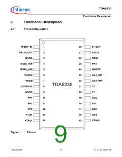
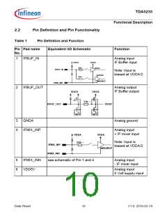
The IC is a low power ASK/FSK Receiver for the frequency bands 300-320, 425-450,
863-870 and 902-928 MHz. Bi-phase modulation schemes, like Manchester, bi-phase
mark, bi-phase space and differential Manchester are supported.
The chip offers best-in-class sensitivity performance at a very high level of integration
and needs only a few external components.
The device is qualified to automotive quality standards and operates between -40 and
+105°C at supply voltage ranges of 3.0-3.6 Volts or 4.5-5.5 Volts.
The receiver is realized as a double down conversion super-heterodyne/low-IF
architecture each with image rejection supplemented by digital signal processing in the
baseband. A fully integrated Sigma-Delta Fractional-N PLL Synthesizer allows for high-
resolution frequency generation and uses a crystal oscillator as the reference. The on-
chip temperature sensor may be utilized for temperature drift compensation via the
crystal oscillator.
The digital baseband processing unit together with the high performance down converter
is the key element for the exceptional sensitivity performance of the device which take it
close to the theoretical top-performance limits. It comprises signal and noise detectors,
matched data filter, clock and data recovery, data slicer and a format decoder. It
demodulates the received ASK or FSK data stream independently and recovers the data
clock out of the received data stream with very fast synchronization times which can then
be either accessed via separate pins or used for further processing like frame
synchronization and intermediate storage in the on-chip FIFO. The RSSI output signal is
converted to the digital domain with an ADC. All these signals are accessible via the 4-
wire SPI interface bus. Up to 2 pre-configured telegram formats can be stored into the
device offering independent pre-processing of the received data to an extent not
available till now. The down converter can be also configured in single-conversion mode
at moderately reduced selectivity performance but at the advantage of omitting the IF
ceramic filter.
Data Sheet
7
V1.0, 2010-02-19

 INFINEON [ Infineon ]