TDA5235
Reference
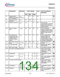
#
Parameter
Symbol
Limit Values
Unit Test Conditions
Remarks
min. typ. max.
C7
Supply current
IRF-FE-
2.2
2.9
mA
■
during RF-FE startup
/ BPF calibration
startup,BPFcal
C8
C9
Brownout detector
threshold
VBOR
tReset
2.3
1.0
2.45
2.6
3.0
V
Receiver reset time
ms
Note: No SPI
communication is allowed
before XOSC start-up is
finished and chip reset is
already finished
C10
C11
Receiver startup
time
tRXstartup
455
111
455
111
455
111
350
µs
µs
Time to startup RF
frontend (comprises time
required to switch crystal
oscillator from Low Power
Mode to High Precision
Mode
■
■
RF Channel Hop
Latency Time and
Configuration (Hop)
Change Latency
Time (e.g. Cfg A to
Cfg B)
tC_Hop
Time to switch RF PLL
between different RF
Channels (does not
include settling of Data
Clock Recovery) and time
to change Configuration
C12
C13
RF Frontend startup tRFstartdelay
delay
350
15
350
12
µs
µs
µs
Delay of startup of RF
frontend
■
■
■
P_ON pulse width
tP_ON
Minimal pulse width to
reset the chip
C14
C15
NINT pulse length
tNINT_Pulse
Pulse width of interrupt
Accuracy of Temperature Sensor
Valid for temperature
range -40°C .. +105°C;
using upper 8 ADC bits
(ADCRESH)
C15.1 uncalibrated
C15.2 calibrated
TError, uncal
TError, cal
+/- 23
°C
uncalibrated (3 sigma)
value
■
■
+/- 4.5 °C
after 1-point calibration at
room temperature (3
sigma)
C16
Accuracy of VDDD readout
Valid for temperature
range -40°C .. +105°C;
using upper 8 ADC bits
(ADCRESH)
C16.1 uncalibrated
C16.2 calibrated
VDDD, Error,
+/- 200 mV
+/- 25 mV
uncalibrated (3 sigma)
value
■
■
uncal
VDDD, Error,
after 1-point calibration at
room temperature (3
sigma)
cal
Data Sheet
134
V1.0, 2010-02-19

 INFINEON [ Infineon ]