TC39x BC/BD-Step
Electrical Specification5 V / 3.3 V switchable Pads
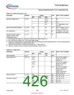
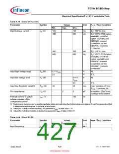
Table 3-12 RFast 3.3V pad (cont’d)
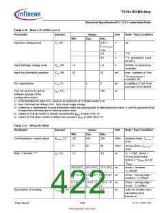
Parameter
Symbol
Values
Typ.
Unit
Note / Test Condition
Min.
Max.
Input low voltage level
VIL SR
-
-
0.42 *
V
AL
VFLEX
-
-
-
-
0.8
0.5
V
V
TTL
TTL (degraded, used
for CIF)
Input low threshold variation
Pin capacitance
V
ILD SR
CIO CC
SET CC
-33
-
33
mV
pF
ns
max. variation of 1ms;
VFLEX = constant; AL
-
-
2
-
3.5
100
in addition 2.5pF from
package to be added
Pad set-up time to get an
software update of the
configuration active
t
1) In the formulas the value of CL needs to be entered in pF to obtain results in ns.
2) Rise / fall times are defined 10% - 90% of pad supply voltage.
3) Hysteresis is implemented to avoid metastable states and switching due to internal ground bounce. It can't be guaranteed that
it suppresses switching due to external system noise.
4) Values for Pull-up resistor is defined via parameter RMDU in table VADC 5V.
5) Values for Pull-down resistor is defined via parameter RMDD in table VADC 5V.
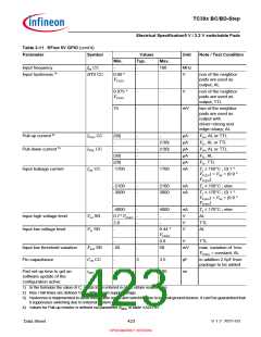
Table 3-13 Class S 5V
Parameter
Symbol
Values
Typ.
Unit
Note / Test Condition
Min.
Max.
160
-
Input frequency
Input hysteresis 1)
fIN CC
-
-
-
MHz
V
HYS CC
0.09 *
VDDM
non of the neighbor
pads are used as
output; AL
0.075 *
VDDM
-
-
-
-
V
non of the neighbor
pads are used as
output; TTL
75
mV
two of the neighbor
pads are used as
output with
driver=strong and
edge=sharp; AL
Pull-up current 2)
I
I
PUH CC
PDL CC
|30|
-
-
-
-
-
-
-
µA
µA
µA
µA
µA
VIH; AL or TTL
VIL; AL or TTL
VIH; AL or TTL
VIL; AL
|130|
Pull-down current 3)
-
|130|
|30|
|28|
-
-
VIL; TTL
Data Sheet
426
V 1.2, 2021-03
OPEN MARKET VERSION

 INFINEON [ Infineon ]