TC39x BC/BD-Step
Pin Definition and Functions: LFBGA-292 Package Variant Pin Configuration
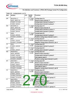
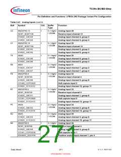
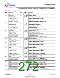
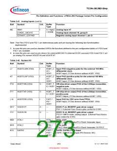
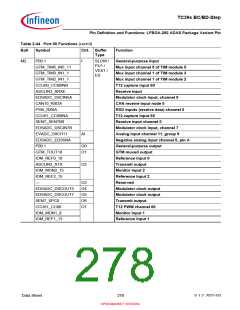
Table 2-42 System I/O (cont’d)
Ball
Symbol
Ctrl. Buffer
Type
Function
L19
TRST
I
I
FAST /
PU2 /
VEXT
JTAG Module Reset/Enable Input
DAPE: DAPE0 Clock Input
DAPE0
K16
J16
TMS
I
FAST /
PD2 /
VEXT
JTAG Module State Machine Control Input
DAP: DAP1 Data I/O
DAP1
I/O
TCK
I
I
FAST /
PD2 /
VEXT
JTAG Module Clock Input
DAP: DAP0 Clock Input
DAP0
G11
G10
G16
DAPE1
DAPE2
ESR1
I/O
I/O
I/O
FAST /
PD2 /
VEXT
DAPE: DAPE1 Data I/O
DAPE: DAPE1 Data I/O (PD Devices: VSS)
FAST /
PD2 /
VEXT
DAPE: DAPE2 Data I/O
DAPE: DAPE2 Data I/O (PD Devices: VSS)
FAST /
PU1 /
VEXT
ESR1 Port Pin input - can be used to trigger a reset or
an NMI
ESR1: External System Request Reset 1. Default NMI
function. See also SCU chapter for details. Default after
power-on can be different. See also SCU chapter ´Reset
Control Unit´ and SCU_IOCR register description.
PMS_EVRWUP: EVR Wakepup Pin
PMS_ESR1WKP
ESR0
I
ESR1 pin input
F16
I/O
FAST /
OD /
ESR0 Port Pin input - can be used to trigger a reset or
an NMI
VEXT
ESR0: External System Request Reset 0. Default
configuration during and after reset is open-drain driver.
The driver drives low during power-on reset. This is valid
additionally after deactivation of PORST_N until the
internal reset phase has finished. See also SCU chapter for
details. Default after power-on can be different. See also
SCU chapter ´Reset Control Unit´ and SCU_IOCR register
description. PMS_EVRWUP: EVR Wakepup Pin
PMS_ESR0WKP
PORST
I
ESR0 pin input
G17
I/O
PORST / PORST pin
PD /
VEXT
Power On Reset Input. Additional strong PD in case of
power fail.
Data Sheet
274
V 1.2, 2021-03
OPEN MARKET VERSION

 INFINEON [ Infineon ]