TC39x BC/BD-Step
Pin Definition and Functions: LFBGA-516 Package Variant Pin Configuration
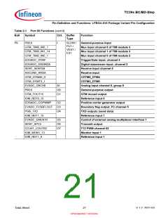
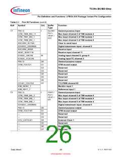
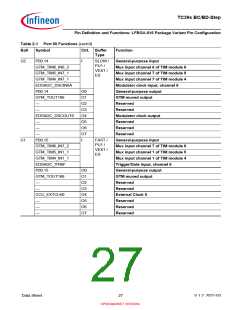
Table 2-1 Port 00 Functions (cont’d)
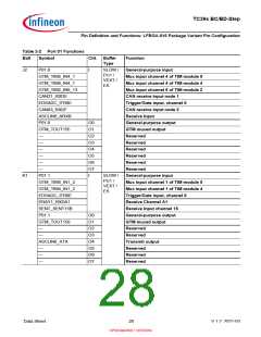
Ball
Symbol
Ctrl. Buffer
Type
Function
R10
P00.10
I
SLOW /
PU1 /
VEXT /
ES1
General-purpose input
Mux input channel 1 of TIM module 4
Mux input channel 1 of TIM module 1
Mux input channel 1 of TIM module 0
Receive input channel 9
Digital datastream input, channel 1
Analog input channel 2, group 9
Positive analog input channel 4, pin B
General-purpose output
GTM muxed output
GTM_TIM4_IN1_11
GTM_TIM1_IN1_1
GTM_TIM0_IN1_1
SENT_SENT9B
EDSADC_DSDIN1A
EVADC_G9CH2
EDSADC_EDS4PB
P00.10
AI
O0
O1
O2
O3
O4
O5
O6
O7
GTM_TOUT19
ASCLIN4_ASCLK
—
Shift clock output
Reserved
—
Reserved
—
Reserved
SENT_SPC9
CCU61_COUT63
IOM_MON1_7
IOM_REF1_7
P00.11
Transmit output
T13 PWM channel 63
Monitor input 1
Reference input 1
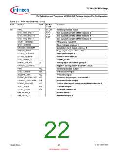
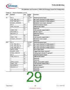
T6
I
SLOW /
PU1 /
VEXT /
ES1
General-purpose input
Mux input channel 2 of TIM module 4
Mux input channel 2 of TIM module 1
Mux input channel 2 of TIM module 0
Trap input capture
GTM_TIM4_IN2_11
GTM_TIM1_IN2_1
GTM_TIM0_IN2_1
CCU60_CTRAPA
EDSADC_DSCIN0A
CCU61_T12HRE
SENT_SENT10B
EVADC_G9CH1
EVADC_FC3CH0
P00.11
Modulator clock input, channel 0
External timer start 12
Receive input channel 10
Analog input channel 1, group 9
Analog input FC channel 3
General-purpose output
GTM muxed output
AI
O0
O1
O2
O3
O4
O5
O6
O7
GTM_TOUT20
ASCLIN4_ASLSO
—
Slave select signal output
Reserved
EDSADC_DSCOUT0
—
Modulator clock output
Reserved
—
Reserved
—
Reserved
Data Sheet
25
V 1.2, 2021-03
OPEN MARKET VERSION

 INFINEON [ Infineon ]