TC39x BC/BD-Step
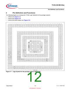
Pin Definition and Functions:
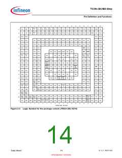
1
2
3
4
5
6
7
8
9
10
11
12
13
14
15
16
17
18
19
20
A
B
C
D
E
F
NC1
VEXT
P10.7
P10.6
P10.2
P10.3
P10.0
P11.11
P11.9
P11.2
P13.3
P13.1
P14.8
P14.5
P14.1
P15.6
P15.4
P15.1
VDDP3
VSS
A
B
C
D
E
F
P02.0
P02.2
P02.4
P02.6
P02.8
P00.0
P00.2
P00.4
P00.7
VSS
VEXT
P10.8
P10.5
P10.4
P10.1
P11.12
P11.10
P11.3
P13.2
P13.0
P14.6
P14.3
P14.4
P14.0
P15.3
VDDP3
VSS
P15.0
P02.1
P02.3
P02.5
P02.7
P00.1
P00.3
P00.5
P00.9
P15.2
P20.14
VSS
VFLEX P11.15
P11.14
P11.8
P11.5
P11.7
P11.6
P11.1
P11.4
P11.0
P14.10
P12.1
P14.9
P12.0
P14.7
P14.2
P15.8
P15.5
P15.7
VDD
VDD
VSS
VSS
P20.9
P20.6
PORST
P20.12 P20.13
P20.10 P20.11
P02.9
VSS
P11.13
P02.11 P02.10
ESR0
ESR1
P20.7
P20.1
P20.2
P21.3
P21.2
TRST
XTAL2
VDD
P20.8
P20.3
P20.0
P21.5
P21.4
VSS
VDDSB
(VDD)
G
H
J
P01.4
P01.6
P00.6
P00.8
AN43
AN41
P01.3
P01.5
P01.7
P00.10
AN42
AN40
VSS
VSS
DAPE2 DAPE1
VSS
VSS
VDD
G
H
J
VDDSB
(VDD)
P21.7 / P21.6 /
TDO
VSS
VSS
VSS
VSS
VSS
VSS
VSS
VSS
VSS
VSS
VSS
VSS
VDD
VSS
TDI
VSS
VSS
VSS
VSS
VSS
VSS
VSS
VSS
VSS
TCK
P21.1
AGBTC
LKP
(VSS)
K
L
VSS
VSS
VSS
VSS
DAPE0
TMS
P21.0
K
L
AGBTC
LKN
(VSS)
AGBTE
RR
(VSS)
P00.11 P00.12
P22.10 P22.11
M
N
P
R
T
AN46
AN44
AN47
AN45
VSS
VDD
VSS
VDD
P22.8
P22.6
P22.4
P23.7
VSS
P22.9
P22.7
P22.5
P23.6
P23.5
VSS
XTAL1
VEXT
P22.0
P22.2
P23.4
P23.2
P23.0
VEXT
M
N
P
R
T
AN36 /
P40.6
AN38 /
P40.8
VSS
VSS
VSS
VSS
AGBTT AGBTT
XN
(VSS)
AN39 /
P40.9
AN37 /
P40.7
AN32 /
P40.4
AN34
AN23
AN22
VDD
XP
(VSS)
VDD
P22.1
P22.3
P23.3
P23.1
VEXT
VSS
AN33 /
P40.5
AN35
AN31
AN30
NC1
VAREF VAGND
2
VEVRS
B
AN15
AN14
AN12
AN9
AN6
AN7
AN4
AN3
AN0
AN1
P34.2
P34.3
P34.4
P34.5
P33.14
P33.15
P32.5
P32.6
2
AN29 /
P40.14 P40.13
AN28 /
AN17 /
P40.10
U
V
W
Y
P34.1
P32.7
U
V
W
Y
AN27 /
P40.3
AN26 /
P40.2
P32.1 /
AN25 /
P40.1
AN24 /
P40.0
AN19 /
P40.12 P40.11
AN18 /
AN16
AN13
AN11
AN8
AN2
P33.0
P33.2
P33.4
P33.6
P33.8
P33.10 P33.12 VGATE
1P
P32.4
P32.0 /
P33.11 P33.13 VGATE
1N
VAREF VAGND
1
NC1
AN21
AN20
VSSM
VDDM
AN10
AN5
P33.1
P33.3
P33.5
P33.7
P33.9
P32.2
P32.3
VSS
1
1
2
3
4
5
6
7
8
9
10
11
12
13
14
15
16
17
18
19
20
TC39xed - (top view)
Figure 2-2 Logic Symbol for the package variant LFBGA-292
Data Sheet
13
V 1.2, 2021-03
OPEN MARKET VERSION

 INFINEON [ Infineon ]