TC1767
Electrical Parameters
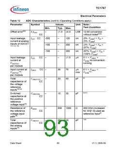
12) Only one of these parameters is tested, the other is verified by design characterization.
13) The leakage current decreases typically 30% for junction temperature decrease of 10oC.
14) Applies to AINx, when used as auxiliary reference inputs.
15) IAREF_MAX is valid for the minimum specified conversion time. The current flowing during an ADC conversion
with a duration of up to tC = 25µs can be calculated with the formula IAREF_MAX = QCONV/tC. Every conversion
needs a total charge of QCONV = 150pC from VAREF
.
All ADC conversions with a duration longer than tC = 25µs consume an IAREF_MAX = 6µA.
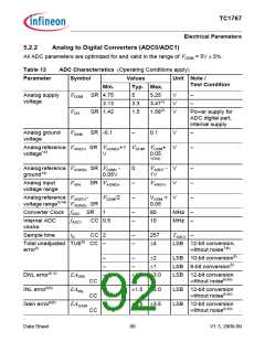
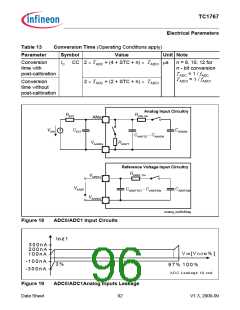
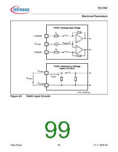
16) For the definition of the parameters see also Figure 18.
17) This represents an equivalent switched capacitance. This capacitance is not switched to the reference voltage
at once. Instead of this smaller capacitances are successively switched to the reference voltage.
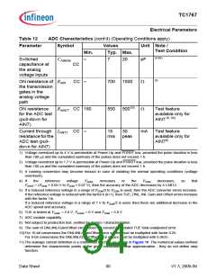
18) The sampling capacity of the conversion C-Network is pre-charged to VAREF/2 before the sampling moment.
Because of the parasitic elements the voltage measured at AINx can deviate from VAREF/2, and is typically
1.35V.
19) RAIN7T = 1400 Ohm maximum and 830 Ohm typical in the VDDM = 3.3V± 5% range.
20) The DC current at the pin is limited to 3 mA for the operational lifetime.
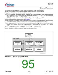
clock
generation
ADC kernel
f
ADC
interrupts,
etc.
divider for
divider for
fADCI
f
ADCD
digital clock
analog clock
f
ADCI
f
ADCD
registers
analog part
arbiter
ADC_clocking
Figure 17
ADC0/ADC1 Clock Circuit
Data Sheet
91
V1.3, 2009-09

 INFINEON [ Infineon ]