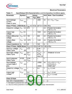
TC1767
Electrical Parameters
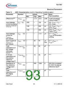
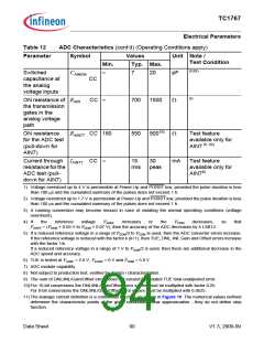
Table 12
ADC Characteristics (cont’d) (Operating Conditions apply)
Parameter
Symbol
Values
Typ. Max.
Unit Note /
Test Condition
Min.
8)18)
Switched
CAINSW
–
7
20
pF
capacitance at
the analog
CC
voltage inputs
8)
ON resistance of RAIN
the transmission
gates in the
CC –
700
1500
Ω
analog voltage
path
ON resistance
for the ADC test
(pull-down for
AIN7)
RAIN7T CC 180
550
90019)
Ω
Test feature
available only for
AIN7 8) 20)
Current through IAIN7T CC –
resistanceforthe
ADC test (pull-
15
rms
30
peak
mA
Test feature
available only for
AIN78)
down for AIN7)
1) Voltage overshoot up to 4 V is permissible at Power-Up and PORST low, provided the pulse duration is less
than 100 µs and the cumulated summary of the pulses does not exceed 1 h.
2) Voltage overshoot up to 1.7 V is permissible at Power-Up and PORST low, provided the pulse duration is less
than 100 µs and the cumulated summary of the pulses does not exceed 1 h.
3) A running conversion may become inexact in case of violating the normal operating conditions (voltage
overshoot).
4) If
the
reference
voltage
VAREF
increases
or
the
VDDM
decreases,
so
that
VAREF = (VDDM + 0.05 V to VDDM + 0.07 V), then the accuracy of the ADC decreases by 4 LSB12.
5) If a reduced reference voltage in a range of VDDM/2 to VDDM is used, then the ADC converter errors increase.
If the reference voltage is reduced with the factor k (k<1), then TUE, DNL, INL Gain and Offset errors increase
with the factor 1/k.
If a reduced reference voltage in a range of 1 V to VDDM/2 is used, then there are additional decrease in the
ADC speed and accuracy.
6) TUE is tested at VAREF = 5.0 V, VAGND = 0 V and VDDM = 5.0 V
7) ADC module capability.
8) Not subject to production test, verified by design / characterization.
9) The sum of DNL/INL/Gain/Offset errors does not exceed the related TUE total unadjusted error.
10) For 10-bit conversions the DNL/INL/Gain/Offset error values must be multiplied with factor 0.25.
For 8-bit conversions the DNL/INL/Gain/Offset error values must be multiplied with 0.0625.
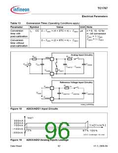
11) The leakage current definition is a continuous function, as shown in Figure 19. The numerical values defined
determine the characteristic points of the given continuous linear approximation - they do not define step
function.
Data Sheet
90
V1.3, 2009-09

 INFINEON [ Infineon ]