TC1767
Introduction
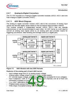
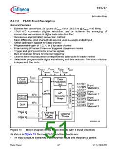
2.4.7.2 FADC Short Description
General Features
• Extreme fast conversion, 21 cycles of fFADC clock (262.5 ns @ fFADC = 80 MHz)
• 10-bit A/D conversion (higher resolution can be achieved by averaging of
consecutive conversions in digital data reduction filter)
• Successive approximation conversion method
• Each differential input channel can also be used as single-ended input
• Offset calibration support for each channel
• Programmable gain of 1, 2, 4, or 8 for each channel
• Free-running (Channel Timers) or triggered conversion modes
• Trigger and gating control for external signals
• Built-in Channel Timers for internal triggering
• Channel timer request periods independently selectable for each channel
• Selectable, programmable digital anti-aliasing and data reduction filter block with four
independent filter units
VDDAF
VFAGND VSSAF
VFAREF
VDDMF VDDIF
VSSMF
fFADC
fCLC
Data
Reduction
Unit
Clock
Control
FAIN0P
FAIN0N
FAIN1P
FAIN1N
FAIN2P
FAIN2N
FAIN3P
FAIN3N
input
channel 0
A/D
Control
input
channel 1
A/D
Converter
Stage
SRx
SRx
Interrupt
Control
input
channel 2
input
channel 3
DMA
TS[H:A]
GS[H:A]
Channel
Trigger
Control
Channel
Timers
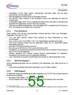
MCB06065_m4
Figure 13
Block Diagram of the FADC Module with 4 Input Channels
As shown in Figure 13, the main FADC functional blocks are:
• An Input Structure containing the differential inputs and impedance control.
Data Sheet
47
V1.3, 2009-09

 INFINEON [ Infineon ]