TC1767
Electrical Parameters
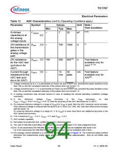
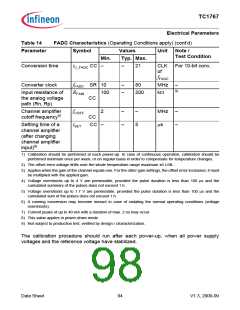
Table 14
FADC Characteristics (Operating Conditions apply) (cont’d)
Parameter
Symbol
Values
Unit Note /
Test Condition
Min.
C_FADC CC –
Typ. Max.
Conversion time
t
–
21
CLK For 10-bit conv.
of
fFADC
Converter clock
fFADC SR 10
–
–
80
MHz
–
9)
Input resistance of
the analog voltage
path (Rn, Rp)
RFAIN
100
200
kΩ
CC
Channel amplifier
cutoff frequency9)
fCOFF
tSET
2
–
–
–
5
MHz
–
–
CC
Settling time of a
channel amplifier
(after changing
channel amplifier
input)9)
CC –
µs
1) Calibration should be performed at each power-up. In case of continuous operation, calibration should be
performed minimum once per week, or on regular basis in order to compensate for temperature changes.
2) The offset error voltage drifts over the whole temperature range maximum ±6 LSB.
3) Applies when the gain of the channel equals one. For the other gain settings, the offset error increases; it must
be multiplied with the applied gain.
4) Voltage overshoots up to 4 V are permissible, provided the pulse duration is less than 100 µs and the
cumulated summary of the pulses does not exceed 1 h.
5) Voltage overshoots up to 1.7 V are permissible, provided the pulse duration is less than 100 µs and the
cumulated sum of the pulses does not exceed 1 h.
6) A running conversion may become inexact in case of violating the normal operating conditions (voltage
overshoots).
7) Current peaks of up to 40 mA with a duration of max. 2 ns may occur
8) This value applies in power-down mode.
9) Not subject to production test, verified by design / characterization.
The calibration procedure should run after each power-up, when all power supply
voltages and the reference voltage have stabilized.
Data Sheet
94
V1.3, 2009-09

 INFINEON [ Infineon ]