TC1767
Electrical Parameters
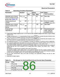
Table 9
Operating Condition Parameters
Symbol Values
Typ. Max.
Parameter
Unit Note /
Test Condition
Min.
Absolute sum of short
circuit currents of a pin
group (see Table 10)
Σ|ISC_PG
|
–
–
20
mA See note
SR
Inactive device pin
current
IID
SR -1
–
–
1
mA All power supply
voltages VDDx = 0
mA See note4)
Absolute sum of short
circuit currents of the
device
Σ|ISC_D
|
–
100
SR
External load
capacitance
CL
SR –
–
–
pF
Dependingonpin
class. See DC
characteristics
1) Digital supply voltages applied to the TC1767 must be static regulated voltages which allow a typical voltage
swing of ±5%.
2) Voltage overshoot up to 1.7 V is permissible at Power-Up and PORST low, provided the pulse duration is less
than 100 µs and the cumulated summary of the pulses does not exceed 1 h.
3) Voltage overshoot up to 4 V is permissible at Power-Up and PORST low, provided the pulse duration is less
than 100 µs and the cumulated summary of the pulses does not exceed 1 h.
4) See additional document “TC1767 Pin Reliability in Overload“ for definition of overload current on digital pins.
5) The overload coupling factor (kA) defines the worst case relation of an overload condition (IOV) at one pin to
the resulting leakage current (IleakTOT) into an adjacent pin: IleakTOT = ±kA × |IOV| + IOZ1.
Thus under overload conditions an additional error leakage voltage (VAEL) will be induced onto an adjacent
analog input pin due to the resistance of the analog input source (RAIN). That means VAEL = RAIN ×
|IleakTOT|.
The definition of adjacent pins is related to their order on the silicon.
The Injected leakage current always flows in the opposite direction from the causing overload current.
Therefore, the total leakage current must be calculated as an algebraic sum of the both component leakage
currents (the own leakage current IOZ1 and the optional injected leakage current).
6) The PLL jitter characteristics add to this value according to the application settings. See the PLL jitter
parameters.
7) Applicable for digital outputs.
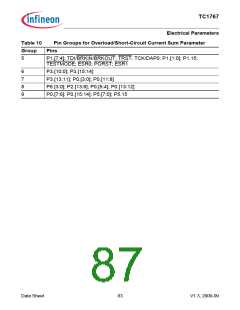
Table 10
Pin Groups for Overload/Short-Circuit Current Sum Parameter
Pins
Group
1
2
3
4
P5.[14:8]
P1.[14:12]; P2.[7:0]
P4.[3:0]
P1.[3:2]; P1.[11:8]
Data Sheet
82
V1.3, 2009-09

 INFINEON [ Infineon ]