TC1767
Electrical Parameters
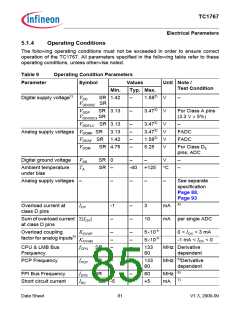
5.1.4
Operating Conditions
The following operating conditions must not be exceeded in order to ensure correct
operation of the TC1767. All parameters specified in the following table refer to these
operating conditions, unless otherwise noted.
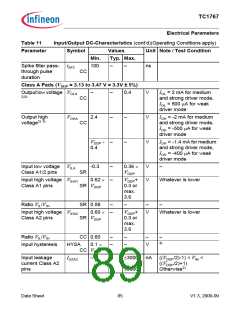
Table 9
Operating Condition Parameters
Symbol Values
Typ. Max.
Parameter
Unit Note /
Test Condition
Min.
Digital supply voltage1) VDD
SR 1.42
–
1.582)
V
V
–
VDDOSC SR
VDDP
SR 3.13
–
3.473)
For Class A pins
V
DDOSC3 SR
(3.3 V ± 5%)
VDDFL3 SR 3.13
Analog supply voltages VDDMF SR 3.13
VDDAF SR 1.42
–
–
–
–
3.473)
3.473)
1.582)
5.25
V
V
V
V
–
FADC
FADC
VDDM
SR 4.75
For Class DE
pins, ADC
Digital ground voltage
VSS
TA
SR 0
SR –
–
–
V
–
–
Ambient temperature
under bias
-40 +125 °C
Analog supply voltages –
–
–
–
–
See separate
specification
Page 88,
Page 93
4)
Overload current at
class D pins
IOV
-1
–
–
–
3
mA
Sum of overload current Σ|IOV|
10
mA per single ADC
at class D pins
Overload coupling
KOVAP
KOVAN
–
–
–
–
–
5×10⁻⁵
5×10⁻⁴
0 < IOV < 3 mA
-1 mA < IOV < 0
factor for analog inputs5)
CPU & LMB Bus
Frequency
fCPU SR
fPCP SR
fSYS SR
–
–
–
133
80
MHz Derivative
dependent
MHz 6)Derivative
dependent
PCP Frequency
–
133
80
6)
FPI Bus Frequency
Short circuit current
–
–
80
+5
MHz
7)
ISC
SR -5
mA
Data Sheet
81
V1.3, 2009-09

 INFINEON [ Infineon ]