TC1767
Introduction
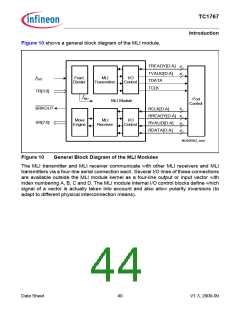
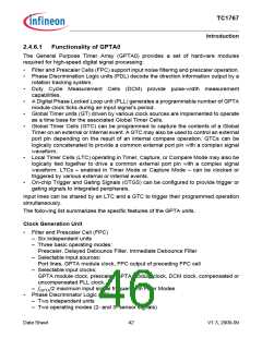
Figure 10 shows a general block diagram of the MLI module.
TREADY[D:A]
4
4
TVALID[D:A]
TDATA
fSYS
Fract.
Divider
MLI
Transmitter
I/O
Control
TCLK
TR[3:0]
fMLI
Port
Control
MLI Module
BRKOUT
SR[7:0]
RCLK[D:A]
4
4
4
4
RREADY[D:A]
RVALID[D:A]
RDATA[D:A]
Move
Engine
MLI
Receiver
I/O
Control
MCB06062_mod
Figure 10
General Block Diagram of the MLI Modules
The MLI transmitter and MLI receiver communicate with other MLI receivers and MLI
transmitters via a four-line serial connection each. Several I/O lines of these connections
are available outside the MLI module kernel as a four-line output or input vector with
index numbering A, B, C and D. The MLI module internal I/O control blocks define which
signal of a vector is actually taken into account and also allow polarity inversions (to
adapt to different physical interconnection means).
Data Sheet
40
V1.3, 2009-09

 INFINEON [ Infineon ]