TC1767
Introduction
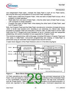
one independent Flash bank, whereas the Data Flash is built of two Flash banks,
allowing the following combinations of concurrent Flash operations:
• Read code or data from Program Flash, while one bank of Data Flash is busy with a
program or erase operation.
• Read data from one bank of Data Flash, while the other bank of Data Flash is busy
with a program or erase operation.
• Program one bank of Data Flash while erasing the other bank of Data Flash, read
from Program Flash.
Both, the Program Flash and the Data Flash, provide error correction of single-bit errors
within a 64-bit read double-word, resulting in an extremely low failure rate. Read
accesses to Program Flash are executed in 256-bit width, to Data Flash in 64-bit width
(both plus ECC). Single-cycle burst transfers of up to 4 double-words and sequential
prefetching with control of prefetch hit are supported for Program Flash.
The minimum programming width is the page, including 256 bytes in Program Flash and
128 bytes in Data Flash. Concurrent programming and erasing in Data Flash is
performed using an automatic erase suspend and resume function.
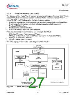
A basic block diagram of the Flash Module is shown in the following figure.
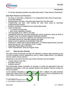
Redundancy
Control
FSI
Voltage Control
Control
Control
Flash Command
State Machine FCS
SFRs
FSRAM
Microcode
Address
Addr Bus
Write Bus
Page
Write
Buffers
256 byte
and
Program
Flash
64
64
WR_DATA
128 byte
8
8
PF-Read
Buffer
256+32 bit
and
ECC Code
Bank 0
Bank 1
ECC Block
Bank 0
Data
Flash
Bank 1
64
DF-Read
Buffer
64+8 bit
Read Bus
64
RD_DATA
Flash Array Module
FAM
Flash Interface&Control Module
FIM
PMU
Flash FSI & Array
Flash_BasicBlockDiagram_generic.vsd
Figure 4
Basic Block Diagram of Flash Module
All Flash operations are controlled simply by transferring command sequences to the
Flash which are based on JEDEC standard. This user interface of the embedded Flash
is very comfortable, because all operations are controlled with high level commands,
such as “Erase Sector”. State transitions, such as termination of command execution, or
errors are reported to the user by maskable interrupts. Command sequences are
Data Sheet
25
V1.3, 2009-09

 INFINEON [ Infineon ]