TC1767
Introduction
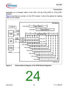
generated on a compare match of the STM with the STM_CMP0 or STM_CMP1
registers.
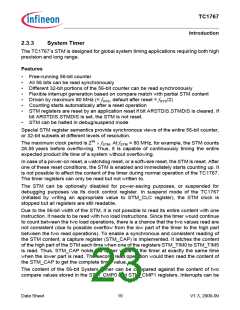
Figure 2 provides an overview on the STM module. It shows the options for reading
parts of STM content.
STM Module
31
23
15
7
0
STM_CMP0
Compare Register 0
to DMA etc.
31
23
15
7
0
STM_CMP1
Compare Register1
STM
IRQ0
55
47
39
31
23
15
7
0
Interrupt
Control
STM
IRQ1
56-bit System Timer
Enable /
Disable
00H
00H
STM_CAP
STM_TIM6
Clock
Control
fSTM
STM_TIM5
STM_TIM4
Address
Decoder
STM_TIM3
STM_TIM2
STM_TIM1
STM_TIM0
PORST
MCB06185_mod
Figure 2
General Block Diagram of the STM Module Registers
Data Sheet
20
V1.3, 2009-09

 INFINEON [ Infineon ]