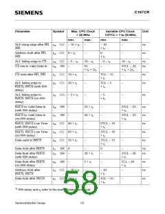
C167CR
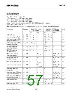
Parameter
Symbol
Max. CPU Clock
= 20 MHz
Variable CPU Clock
1/2TCL = 1 to 20 MHz
Unit
min.
max.
min.
max.
ALE rising edge after RD, t26 CC – 10 + tF
WR
–
– 10
+ tF
–
ns
ns
Address hold after RD,
WR
t28 CC 0 + tF
–
0
+ tF
–
ALE falling edge to CS
CS low to Valid Data In
t38 CC – 5 – tA
10 – tA
–5 – tA
10 – tA
ns
ns
t39 SR
–
55
–
3TCL – 20
+ tC + 2tA
+ tC + 2tA
CS hold after RD, WR
t41 CC 10 + tF
t42 CC 20 + tA
–
–
TCL – 15
+ tF
–
–
ns
ns
ALE falling edge to
RdCS, WrCS (with RW-
delay)
TCL – 5
+ tA
ALE falling edge to
RdCS, WrCS (no RW-
delay)
t43 CC – 5 + tA
–
– 5
+ tA
–
ns
RdCS to Valid Data In
(with RW-delay)
t46 SR
t47 SR
–
–
25 + tC
–
–
2TCL – 25
+ tC
ns
ns
ns
ns
ns
RdCS to Valid Data In
(no RW-delay)
50 + tC
3TCL – 25
+ tC
RdCS, WrCS Low Time
(with RW-delay)
t48 CC 40 + tC
t49 CC 65 + tC
t50 CC 35 + tC
–
–
–
2TCL – 10
+ tC
–
–
–
–
RdCS, WrCS Low Time
(no RW-delay)
3TCL – 10
+ tC
Data valid to WrCS
2TCL – 15
+ tC
Data hold after RdCS
t51 SR
t53 SR
0
–
–
0
–
ns
ns
Data float after RdCS
(with RW-delay)
30 + tF
2TCL – 20
+ tF
Data float after RdCS
(no RW-delay)
t68 SR
–
5 + tF
–
TCL – 20
+ tF
ns
ns
ns
Address hold after
RdCS, WrCS
t55 CC – 10 + tF
t57 CC 10 + tF
–
–
– 10
+ tF
–
–
Data hold after WrCS
TCL – 15
+ tF
1)
RW-delay and tA refer to the next following bus cycle.
Semiconductor Group
55

 INFINEON [ Infineon ]