S29GL01GP
S29GL512P
S29GL256P
S29GL128P
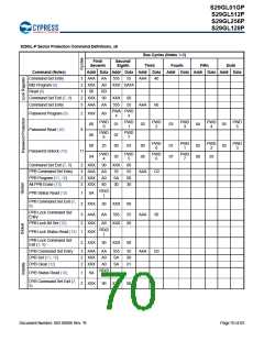
Legend
X = Don’t care
RA = Address of the memory to be read.
RD = Data read from location RA during read operation.
PA = Address of the memory location to be programmed. Addresses latch on the falling edge of the WE# or CE# pulse, whichever happens
later.
PD = Data to be programmed at location PA. Data latches on the rising edge of the WE# or CE# pulse, whichever happens first.
SA = Address of the sector to be verified (in autoselect mode) or erased. Address bits Amax–A16 uniquely select any sector.
WBL = Write Buffer Location. The address must be within the same write buffer page as PA.
WC = Word Count is the number of write buffer locations to load minus 1.
Notes
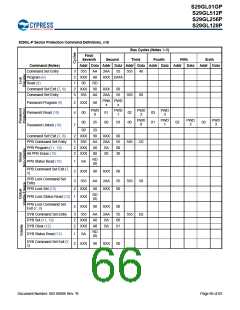
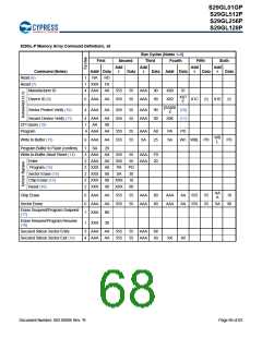
1. See Table on page 15 for description of bus operations.
2. All values are in hexadecimal.
3. All bus cycles are write cycles unless otherwise noted.
4. Data bits DQ15-DQ8 are don’t cares for unlock and command cycles.
5. Address bits AMAX:A16 are don’t cares for unlock and command cycles, unless SA or PA required. (AMAX is the Highest Address pin.).
6. No unlock or command cycles required when reading array data.
7. The Reset command is required to return to reading array data when device is in the autoselect mode, or if DQ5 goes high (while the
device is providing status data).
8. See Table on page 18 for device ID values and definitions.
9. The fourth, fifth, and sixth cycles of the autoselect command sequence are read cycles.
10.The data is 00h for an unprotected sector and 01h for a protected sector. See Autoselect on page 17 for more information. This is same as
PPB Status Read except that the protect and unprotect statuses are inverted here.
11.The data value for DQ7 is “1” for a serialized, protected Secured Silicon Sector region and “0” for an unserialized, unprotected region. See
Table on page 18 for data and definitions.
12.Command is valid when device is ready to read array data or when device is in autoselect mode.
13.Depending on the number of words written, the total number of cycles may be from 6 to 69.
14.Command sequence returns device to reading array after being placed in a Write-to-Buffer-Abort state. Full command sequence is
required if resetting out of abort while in Unlock Bypass mode.
15.The Unlock-Bypass command is required prior to the Unlock-Bypass-Program command.
16.The Unlock-Bypass-Reset command is required to return to reading array data when the device is in the unlock bypass mode.
17.The system can read and program/program suspend in non-erasing sectors, or enter the autoselect mode, when in the Erase Suspend
mode. The Erase Suspend command is valid only during a sector erase operation.
18.The Erase Resume/Program Resume command is valid only during the Erase Suspend/Program Suspend modes.
19.The Exit command returns the device to reading the array.
Document Number: 002-00886 Rev. *B
Page 69 of 83

 INFINEON [ Infineon ]