OptiMOSTM5ꢀPower-Transistor,ꢀ60ꢀV
ISZ0703NLS
1ꢀꢀꢀꢀꢀMaximumꢀratings
atꢀTA=25ꢀ°C,ꢀunlessꢀotherwiseꢀspecified
Tableꢀ2ꢀꢀꢀꢀꢀMaximumꢀratings
Values
Typ.
Parameter
Symbol
Unit Noteꢀ/ꢀTestꢀCondition
Min.
Max.
VGS=10ꢀV,ꢀTC=25ꢀ°C
VGS=10ꢀV,ꢀTC=100ꢀ°C
-
-
-
-
-
-
56
39
13
Continuous drain current1)
ID
A
VGS=10ꢀV,ꢀTA=25ꢀ°C,
RTHJA=60ꢀ°C/W2)
Pulsed drain current3)
Avalanche energy, single pulse4)
ID,pulse
EAS
-
-
-
-
224
21
A
TA=25ꢀ°C
-
mJ
V
ID=20ꢀA,ꢀRGS=25ꢀΩ
Gate source voltage
VGS
-20
20
-
-
-
-
-
44
2.5
TC=25ꢀ°C
Power dissipation
Ptot
W
TA=25ꢀ°C,ꢀRTHJA=60ꢀ°C/W2)
IEC climatic category; DIN IEC 68-1:
55/175/56
Operating and storage temperature
Tj,ꢀTstg
-55
-
175
°C
2ꢀꢀꢀꢀꢀThermalꢀcharacteristics
Tableꢀ3ꢀꢀꢀꢀꢀThermalꢀcharacteristics
Values
Typ.
Parameter
Symbol
Unit Noteꢀ/ꢀTestꢀCondition
Min.
Max.
Thermal resistance, junction - case,
bottom
RthJC
RthJC
RthJA
-
2.5
3.4
°C/W -
°C/W -
°C/W -
Thermal resistance, junction - case,
top
-
-
-
-
20
60
Device on PCB,
6 cm² cooling area 2)
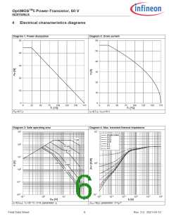
1) Rating refers to the product only with datasheet specified absolute maximum values, maintaining case temperature
as specified. For other case temperatures please refer to Diagram 2. De-rating will be required based on the actual
environmental conditions.
2) Device on 40 mm x 40 mm x 1.5 mm epoxy PCB FR4 with 6 cm2 (one layer, 70 µm thick) copper area for drain
connection. PCB is vertical in still air.
3) See Diagram 3 for more detailed information
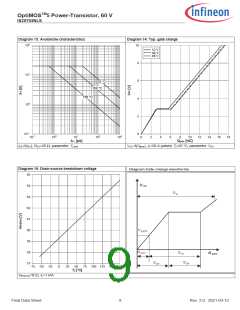
4) See Diagram 13 for more detailed information
Final Data Sheet
3
Rev.ꢀ2.0,ꢀꢀ2021-03-12

 INFINEON [ Infineon ]