CoolSET®-F3R
ICE3BR0665JF
Electrical Characteristics
4.3.6
Current Limiting
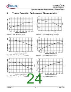
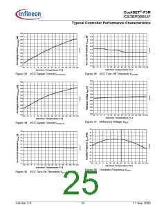
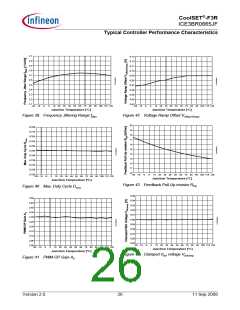
Parameter
Symbol
Limit Values
Unit
Test Condition
min.
typ.
max.
Peak Current Limitation
(incl. Propagation Delay)
Vcsth
0.88
1.06
1.13
V
dVsense / dt = 0.6V/µs
(see Figure 13)
Peak Current Limitation during VCS2
0.22
-
0.26
220
-0.2
0.29
V
Active Burst Mode
Leading Edge Blanking
tLEB
-
-
ns
µA
CS Input Bias Current
ICSbias
-1.5
VCS =0V
4.3.7
CoolMOS® Section
Parameter
Symbol
Limit Values
Unit
Test Condition
min.
typ.
max.
Drain Source Breakdown Voltage
V(BR)DSS 650
-
-
V
Tj = 110°C1) (Refer to
Figure 65 for other
V
(BR)DSS in different Tj)
VGS=0V, ID=0.25mA
VGS=0V, ID=4.8A
Drain Source Avalanche
Breakdown Voltage
V(BR)DS
RDSon
-
700
-
V
Drain Source On-Resistance
-
-
-
0.59
1.31
1.60
0.66
1.46
1.79
Ω
Ω
Ω
Tj = 25°C
Tj=125°C1)
Tj=150°C1)
at ID = 4.5A
Effective output capacitance,
energy related
Co(er)
-
34
-
pF
V
DS = 0V to 480V1)
Rise Time
Fall Time
1)
trise
tfall
-
-
302)
302)
-
-
ns
ns
The parameter is not subjected to production test - verified by design/characterization
Measured in a Typical Flyback Converter Application
2)
Version 2.0
23
11 Sep 2008

 INFINEON [ Infineon ]