IAUC60N04S6L030H
Values
typ.
Parameter
Symbol
Conditions
Unit
min.
max.
Dynamic characteristics2)
Input capacitance
Output capacitance
Reverse transfer capacitance
Turn-on delay time
Rise time
C iss
C oss
Crss
t d(on)
t r
-
-
-
-
-
-
-
1637
458
29
3
2128 pF
596
VGS=0V, VDS=25V,
f =1MHz
44
-
-
-
-
ns
2
VDD=20V, VGS=10V,
I D=60A, R G=3.5W
t d(off)
t f
Turn-off delay time
Fall time
16
8
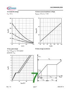
Gate Charge Characteristics2)
Gate to source charge
Gate to drain charge
Gate charge total
Q gs
-
-
-
-
5.0
5.2
27
6.6
7.9
35
-
nC
Q gd
VDD=32V, I D=60A,
VGS=0 to 10V
Q g
Vplateau
Gate plateau voltage
3.0
V
A
Reverse Diode
Diode continous forward current2)
Diode pulse current2)
I S
T C=25°C
-
-
-
-
75
I S,pulse
T C=25°C, t p =100µs
341
VGS=0V, I F=30A,
T j=25°C
VSD
Diode forward voltage
Reverse recovery time2)
-
-
-
0.8
30
18
1.1
V
VR=20V, I F=50A,
diF/dt =100A/µs
t rr
-
-
ns
nC
Reverse recovery charge2)
Q rr
1)
Practically the current is limited by overall system design including customer specific PCB.
2) The parameter is not subject to production test - specified by design.
3) The product can operate at specified current based on best practice to minimize electromigration at the solder joint.
For rare events and inrush currents the value may be exceeded.
4) Device on 2s2p FR4 PCB defined in accordance with JEDEC standards (JESD51-5, -7). PCB is vertical in still air.
Rev. 1.0
page 3
2020-09-18

 INFINEON [ Infineon ]