AIROC™ Bluetooth® system on chip for automotive applications
Table of contents
Table of contents
Features ...........................................................................................................................................1
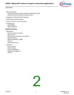
Applications......................................................................................................................................2
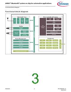
Functional block diagram...................................................................................................................3
Table of contents...............................................................................................................................4
1 Bluetooth® baseband core ...............................................................................................................6
1.1 BQB and regulatory testing support ......................................................................................................................6
1.2 Wi-Fi coexistence support ......................................................................................................................................7
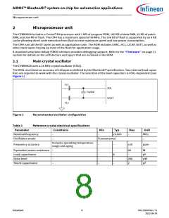
2 Microprocessor unit ........................................................................................................................8
2.1 Main crystal oscillator.............................................................................................................................................8
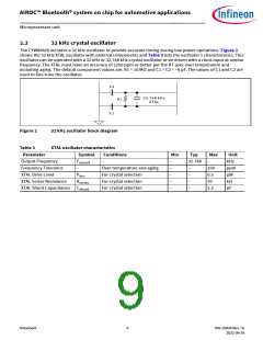
2.2 32 kHz crystal oscillator..........................................................................................................................................9
2.3 Low-frequency clock sources...............................................................................................................................10
2.4 Power modes ........................................................................................................................................................11
2.5 Watchdog ..............................................................................................................................................................11
2.6 Lockout functionality............................................................................................................................................11
2.7 True random number generator ..........................................................................................................................11
3 Power-on and external reset..........................................................................................................12
4 Power management unit ...............................................................................................................13
5 Power configurations....................................................................................................................14
5.1 Configuration 1 - VBAT and VDDIO.......................................................................................................................14
5.2 Configuration 2 - External supplies......................................................................................................................15
5.3 Configuration 3 - LDOs and VDDIO.......................................................................................................................15
6 Integrated radio transceiver ..........................................................................................................16
6.1 Transmitter path...................................................................................................................................................16
6.1.1 Digital modulator...............................................................................................................................................16
6.1.2 Power amplifier..................................................................................................................................................16
6.2 Receiver path ........................................................................................................................................................16
6.2.1 Digital demodulator and bit synchronizer........................................................................................................16
6.2.2 Receiver signal strength indicator ....................................................................................................................16
6.3 Local oscillator......................................................................................................................................................16
7 Peripherals ..................................................................................................................................17
7.1 I2C compatible master .........................................................................................................................................17
7.2 Serial peripheral interface....................................................................................................................................17
7.3 HCI UART interface................................................................................................................................................17
7.4 Peripheral UART interface ....................................................................................................................................17
7.5 GPIO ports .............................................................................................................................................................17
7.6 ADC ........................................................................................................................................................................18
7.7 PWM .......................................................................................................................................................................18
7.8 PDM microphone ..................................................................................................................................................19
7.9 I2S interface ..........................................................................................................................................................19
7.10 PCM interface ......................................................................................................................................................19
7.10.1 Slot mapping....................................................................................................................................................19
7.10.2 Frame synchronization....................................................................................................................................20
7.10.3 Data formatting................................................................................................................................................20
8 Firmware .....................................................................................................................................21
9 Pin assignments and GPIOs............................................................................................................22
10 Ball maps ...................................................................................................................................31
10.1 48-pin WQFN pin map.........................................................................................................................................31
11 Specifications .............................................................................................................................32
11.1 Electrical characteristics ....................................................................................................................................32
11.2 Brown out............................................................................................................................................................33
11.2.1 Core buck regulator .........................................................................................................................................33
Datasheet
4
002-25826 Rev. *G
2022-09-24

 INFINEON [ Infineon ]