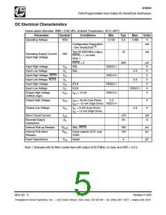
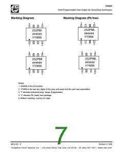
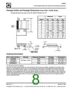
ICS252
Field Programmable Dual Output SS VersaClock Synthesizer
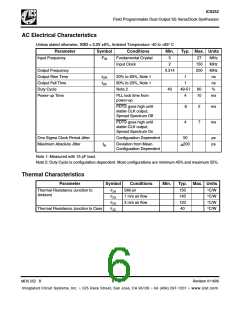
AC Electrical Characteristics
Unless stated otherwise, VDD = 3.3V 5%, Ambient Temperature -40 to +85° C
Parameter
Symbol
Conditions
Fundamental Crystal
Input Clock
Min.
5
Typ. Max. Units
Input Frequency
F
27
MHz
MHz
MHz
ns
IN
2
150
200
Output Frequency
Output Rise Time
Output Fall Time
Duty Cycle
0.314
t
20% to 80%, Note 1
80% to 20%, Note 1
Note 2
1
1
OR
t
ns
OF
40
49-51
4
60
10
%
Power-up Time
PLL lock time from
power-up
ms
PDTS goes high until
stable CLK output,
Spread Spectrum Off
.6
4
2
7
ms
ms
PDTS goes high until
stable CLK output,
Spread Spectrum On
One Sigma Clock Period Jitter
Maximum Absolute Jitter
Configuration Dependent
50
ps
ps
t
Deviation from Mean.
+200
ja
Configuration Dependent
Note 1: Measured with 15 pF load.
Note 2: Duty Cycle is configuration dependent. Most configurations are minimum 45% and maximum 55%.
Thermal Characteristics
Parameter
Symbol
Conditions
Min.
Typ. Max. Units
Thermal Resistance Junction to
Ambient
θ
θ
θ
Still air
150
140
120
40
°C/W
°C/W
°C/W
°C/W
JA
JA
JA
JC
1 m/s air flow
3 m/s air flow
Thermal Resistance Junction to Case
θ
MDS 252 B
6
Revision 011606
Integrated Circuit Systems, Inc. ● 525 Race Street, San Jose, CA 95126 ● tel (408) 297-1201 ● www.icst.com

 IDT [ INTEGRATED DEVICE TECHNOLOGY ]