ICS252
Field Programmable Dual Output SS VersaClock Synthesizer
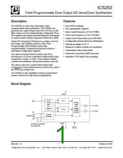
Pin Assignment
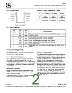
Output Clock Selection Table
S1
CLK1 (MHz) CLK2 (MHz)
Spread
Percentage
User
Configurable
User
S E L
V D D
1
2
3
4
8
7
6
5
P D T S
G N D
0
User
User
Configurable
User
Configurable
User
X 1 / I C L K
X 2
C L K 2
C L K 1
0
Configurable
Configurable
Configurable
8-pin (150 mil) SOIC
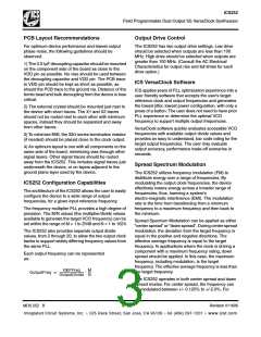
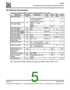
Pin Descriptions
Pin
Number
Pin
Name
Pin
Pin Description
Type
Input
Power
XI
1
2
3
4
5
6
7
SEL
Select pin for frequency selection on CLK1 and CLK2. Internal pull-up resistor.
Connect to +3.3 V.
VDD
X1/ICLK
X2
Connect this pin to a crystal or external clock input.
Connect this pin to a crystal, or float for clock input.
XO
CLK1
CLK2
GND
Output Clock1 output. Weak internal pull-down when tri-stated.
Input
Clock2 output. Weak internal pull-down when tri-stated.
Connect this to ground.
Power
Powers down entire chip. Tri-states CLK outputs when low. Internal pull-up
resistor.
8
PDTS
Input
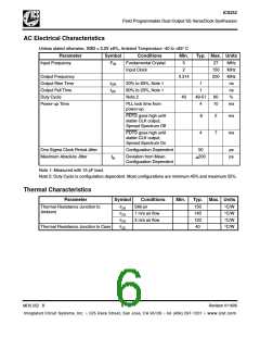
External Components
The ICS252 requires a minimum number of external
components for proper operation.
Crystal Load Capacitors
The device crystal connections should include pads for
small capacitors from X1 to ground and from X2 to
ground. These capacitors are used to adjust the stray
capacitance of the board to match the nominally
required crystal load capacitance. Because load
capacitance can only be increased in this trimming
process, it is important to keep stray capacitance to a
minimum by using very short PCB traces (and no vias)
been the crystal and device. Crystal capacitors must be
connected from each of the pins X1 and X2 to ground.
Series Termination Resistor
Clock output traces over one inch should use series
termination. To series terminate a 50Ω trace (a
commonly used trace impedance), place a 33Ω resistor
in series with the clock line, as close to the clock output
pin as possible. The nominal impedance of the clock
output is 20Ω.
Decoupling Capacitor
The value (in pF) of these crystal caps should equal
As with any high-performance mixed-signal IC, the
ICS252 must be isolated from system power supply
noise to perform optimally.
(C -6 pF)*2. In this equation, C = crystal load
L
L
capacitance in pF. Example: For a crystal with a 16 pF
load capacitance, each crystal capacitor would be 20
pF [(16-6) x 2] = 20.
A decoupling capacitor of 0.01µF must be connected
between VDD and the PCB ground plane.
MDS 252 B
2
Revision 011606
Integrated Circuit Systems, Inc. ● 525 Race Street, San Jose, CA 95126 ● tel (408) 297-1201 ● www.icst.com

 IDT [ INTEGRATED DEVICE TECHNOLOGY ]