®
IS42S81600A, IS42S16800A, IS42S32400A
IS42LS81600A, IS42LS16800A, IS42LS32400A
ISSI
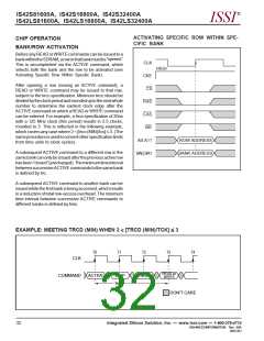
READS
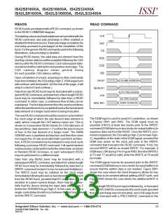
READ COMMAND
READburstsareinitiatedwithaREADcommand,asshown
in the READ COMMAND diagram.
CLK
CKE
Thestartingcolumnandbankaddressesareprovidedwiththe
READ command, and auto precharge is either enabled or
disabledforthatburstaccess.Ifautoprechargeisenabled,the
row being accessed is precharged at the completion of the
burst.ForthegenericREADcommandsusedinthefollowing
illustrations, auto precharge is disabled.
HIGH
CS
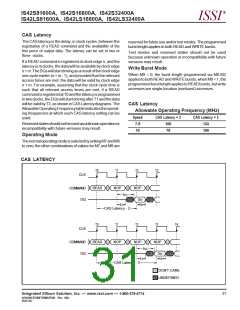
During READ bursts, the valid data-out element from the
startingcolumnaddresswillbeavailablefollowingtheCAS
latencyaftertheREADcommand. Eachsubsequent data-
outelementwillbevalidbythenextpositiveclockedge.The
CAS Latency diagram shows general timing
for each possible CAS latency setting.
RAS
CAS
WE
Upon completion of a burst, assuming no other commands
havebeeninitiated,theDQswillgoHigh-Z.Afull-pageburst
will continue until terminated. (At the end of the page, it will
wrap to column 0 and continue.)
COLUMN ADDRESS
AUTO PRECHARGE
A0-A7
A8, A9, A11
A10
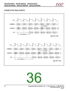
Data from any READ burst may be truncated with a subse-
quentREADcommand, anddatafromafixed-lengthREAD
burst may be immediately followed by data from a READ
command. In either case, a continuous flow of data can be
maintained.Thefirstdataelementfromthenewburstfollows
eitherthelastelementofacompletedburstorthelastdesired
data element of a longer burst which is being truncated.
NO PRECHARGE
BANK ADDRESS
BA0, BA1
ThenewREADcommandshouldbeissuedxcyclesbefore
the clock edge at which the last desired data element is
valid, where x equals the CAS latency minus one. This is
shown in Consecutive READ Bursts for CAS latencies of
twoandthree;dataelementn+3iseitherthelastofaburst
of four or the last desired of a longer burst. The 64Mb
SDRAM uses a pipelined architecture and therefore does
not require the 2n rule associated with a prefetch architec-
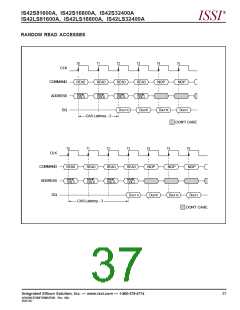
ture. AREADcommandcanbeinitiatedonanyclockcycle
following a previous READ command. Full-speed random
readaccessescanbeperformedtothesamebank,asshown
in Random READ Accesses, or each subsequent READ
may be performed to a different bank.
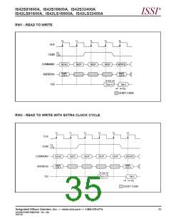
The DQM input is used to avoid I/O contention, as shown
in Figures RW1 and RW2. The DQM signal must be
asserted (HIGH) at least two clocks prior to the WRITE
command(DQMlatencyistwoclocksforoutputbuffers)to
suppress data-out from the READ. Once the WRITE com-
mandisregistered,theDQswillgoHigh-Z(orremainHigh-
Z), regardless of the state of the DQM signal, provided the
DQM was active on the clock just prior to the WRITE
command that truncated the READ command. If not, the
second WRITE will be an invalid WRITE. For example, if
DQMwasLOWduringT4inFigureRW2,thentheWRITEs
at T5 and T7 would be valid, while the WRITE at T6 would
be invalid.
Data from any READ burst may be truncated with a
subsequent WRITE command, and data from a fixed-length
READ burst may be immediately followed by data from a
WRITE command (subject to bus turnaround limitations).
The WRITE burst may be initiated on the clock edge
immediatelyfollowingthelast(orlastdesired)dataelement
from the READ burst, provided that I/O contention can be
avoided. In a given system design, there may be a possi-
bility that the device driving the input data will go Low-Z
before the SDRAM DQs go High-Z. In this case, at least a
single-cycledelayshouldoccurbetweenthelastreaddata
and the WRITE command.
The DQM signal must be de-asserted prior to the WRITE
command (DQM latency is zero clocks for input buffers) to
ensure that the written data is not masked. Figure RW1
shows the case where the clock frequency allows for bus
contention to be avoided without adding a NOP cycle, and
Figure RW2 shows the case where the additional NOP is
needed.
Afixed-lengthREADburstmaybefollowedby, ortruncated
with, aPRECHARGEcommandtothesamebank(provided
that auto precharge was not activated), and a full-page burst
may be truncated with a PRECHARGE command to the
Integrated Silicon Solution, Inc. — www.issi.com — 1-800-379-4774
ADVANCEDINFORMATION Rev. 00A
33
06/01/02

 ICSI [ INTEGRATED CIRCUIT SOLUTION INC ]