IC80C51
IC80C31
t
CLCX
tCHCX
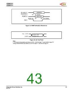
Vcc — 0.5V
0.45V
0.7Vcc
0.2Vcc — 0.1
t
CHCL
tCLCH
t
CLCL
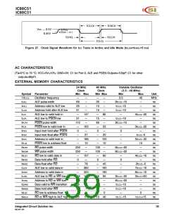
Figure 27. Clock Signal Waveform for ICC Tests in Active and Idle Mode (tCLCH=tCHCL=5 ns)
AC CHARACTERISTICS
(Ta=0°C to 70 °C; VCC=5V+10ꢀ; GND=0V; C1 for Port 0, ALE and PSEN Outputs=100pF; C1 for other
outputs=80pF)
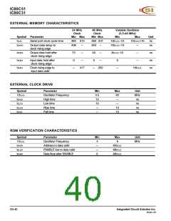
EXTERNAL MEMORY CHARACTERISTICS
24 MHz
Clock
Min Max
40 MHz
Clock
Min Max
Variable Oscillator
(3.5 - 40 MHz)
Symbol Parameter
Min
3.5
Max
Unit
MHz
ns
ns
ns
ns
ns
ns
ns
ns
ns
ns
ns
ns
ns
ns
ns
ns
ns
ns
ns
ns
ns
ns
ns
ns
1/tCLCL
tLHLL
tAVLL
tLLAX
tLLIV
Oscillator frequency
—
68
26
31
—
31
110
—
0
—
—
—
35
10
15
—
15
60
—
0
—
—
40
ALE pulse width
2tCLCL–15
tCLCL–15
tCLCL–10
—
—
Address valid to ALE low
Address hold after ALE low
ALE low to valid instr in
ALE low to PSEN low
PSEN pulse width
—
—
—
—
—
—
147
—
80
—
4tCLCL–20
—
tLLPL
tCLCL–10
3tCLCL–15
—
tPLPH
tPLIV
—
—
—
PSEN low to valid instr in
Input instr hold after PSEN
Input instr float after PSEN
Address to valid instr in
PSEN low to address float
RD pulse width
105
—
55
—
3tCLCL–20
—
tPXIX
0
tPXIZ
—
—
—
230
230
—
0
37
—
—
—
130
130
—
0
20
105
10
—
—
tCLCL–5
5tCLCL–20
10
tAVIV
188
10
—
tPLAZ
tRLRH
tWLWH
tRLDV
tRHDX
tRHDZ
tLLDV
tAVDV
tLLWL
tAVWL
tQVWX
tWHQX
tRLAZ
tWHLH
—
—
6tCLCL–20
6tCLCL–20
—
—
WR pulse width
—
—
—
RD low to valid data in
Data hold after RD
157
—
90
—
4tCLCL–10
—
0
Data float after RD
—
—
—
78
—
—
—
45
165
190
—
2tCLCL–5
7tCLCL–10
8tCLCL–10
3tCLCL+20
—
ALE low to valid data in
Address to valid data in
ALE low to RD or WR low
Address to RD or WR low
Data valid to WR transition
Data hold after WR
282
323
—
—
105 145
55 95
3tCLCL–20
4tCLCL–20
tCLCL–15
tCLCL–10
—
146
26
31
—
—
—
—
0
80
10
15
—
—
—
—
0
—
—
RD low to address float
RD or WR high to ALE high
0
26
57
10 40
tCLCL–15
tCLCL+15
Integrated Circuit Solution Inc.
MC001-0B
39

 ICSI [ INTEGRATED CIRCUIT SOLUTION INC ]