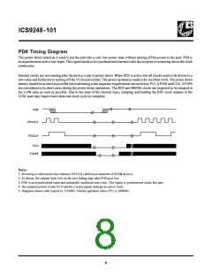
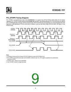
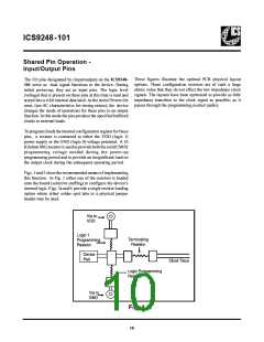
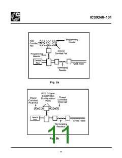
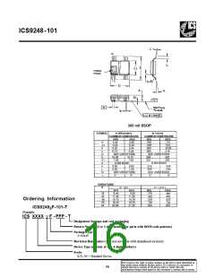
ICS9248-101
Absolute Maximum Ratings
Supply Voltage. . . . . . . . . . . . . . . . . . . . . . . . . . . 7.0 V
Logic Inputs . . . . . . . . . . . . . . . . . . . . . . . . . . . . . GND 0.5 V to VDD +0.5 V
Ambient Operating Temperature . . . . . . . . . . . . 0°C to +70°C
Case Temperature . . . . . . . . . . . . . . . . . . . . . . . . 115°C
Storage Temperature . . . . . . . . . . . . . . . . . . . . . . 65°C to +150°C
Stresses above those listed under Absolute Maximum Ratings may cause permanent damage to the device.These ratings are stress
specifications only and functional operation of the device at these or any other conditions above those listed in the operational
sections of the specifications is not implied. Exposure to absolute maximum rating conditions for extended periods may affect
product reliability.
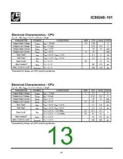
Electrical Characteristics - Input/Supply/Common Output Parameters
TA = 0 - 70C; Supply Voltage VDD = VDDL = 3.3 V +/-5% (unless otherwise stated)
PARAMETER
Input High Voltage
Input Low Voltage
SYMBOL
VIH
CONDITIONS
MIN
2
TYP
MAX UNITS
VDD+0.3
0.8
V
V
VIL
VSS-0.3
CL = 0 pF; Select @ 66MHz
CL = 0 pF; Select @ 100MHz
CL = 0 pF; Select @ 133MHz
90
150
Operating Supply
Current
IDD3.3OP
mA
120
151
170
180
IDDP D
Fi
µA
Powerdown Current
Input Frequency
Input Capacitance1
CL = 0 pF; Input address VDD or GND
VDD = 3.3 V
250
600
16
12
27
14.318
MHz
CIN
Logic Inputs
X1 & X2 pins
5
pF
pF
CINX
36
45
Clk Stabilization1
Skew1
TSTAB
From VDD = 3.3 V to 1% target Freq.
5.5
4
ms
ns
tCP U-P CI1 VT = 1.5 V
1
2.8
1Guaranteed by design, not 100% tested in production.
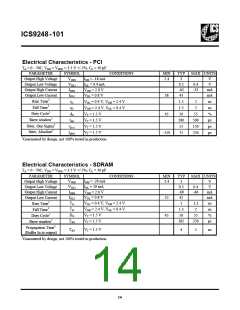
Electrical Characteristics - Input/Supply/Common Output Parameters
TA = 0 - 70º C; Supply Voltage VDD = 3.3 V +/-5%, VDDL = 2.5 V +/-5% (unless otherwise stated)
PARAMETER
SYMBOL
CONDITIONS
MIN
TYP
8
MAX UNITS
15
CL = 0 pF; Select @ 66.8 MHz
CL = 0 pF; Select @ 100 MHz
CL = 0 pF; Select @ 133 MHz
Operating SupplyCurrent
IDDL2.5
mA
11
18
20
10
17
IDDLP D
Powerdown Current
Skew1
<1
2.4
A
µ
CL = 0 pF; Input address VDD or GND
VT = 1.5 V; VTL = 1.25 V
tCP U-P CI2
1
4
ns
1Guaranteed by design, not 100% tested in production.
12

 ICSI [ INTEGRATED CIRCUIT SOLUTION INC ]