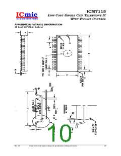
ICM7115
LOW COST SINGLE CHIP TELEPHONE IC
WITH VOLUME CONTROL
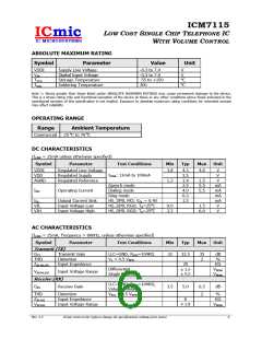
ABSOLUTE MAXIMUM RATING
Symbol
Parameter
Value
Unit
VDDI
VIN_
TSTG
TSOL
Supply Line Voltage
-0.3 to 7.0
V
V
Digital Input Voltage
Storage Temperature
Soldering Temperature
-0.3 to 7.0
-55 to +150
300
oC
oC
Note 1: Stress greater than those listed under ABSOLUTE MAXIMUM RATINGS may cause permanent damage to the device.
This is a stress rating only and functional operation of the device at these or any other conditions above those indicated in the
operational sections of this specification is not implied. Exposure to absolute maximum rating conditions for extended periods
may affect reliability.
OPERATING RANGE
Range
Ambient Temperature
Commercial -25 oC to 70 oC
DC CHARACTERISTICS
(ILINE = 15mA unless otherwise specified)
Symbol
Parameter
Test Conditions
Min
Typ
Max
Unit
VDDI
VDD
AGND
Regulated Line Voltage
Regulated Supply
Regulated Reference
3.8
4.3
3.5
1.4
2.5
4.0
0.3
1.5
4.6
V
V
V
mA
mA
mA
mA
V
ILINE: 13mA to 100mA
1.3
1.5
5.5
5.5
Speech mode
Dialing mode
Ring mode
HS_DPB, MO; VOL = 0.4V
HS_DPB, RGD; TA=25oC
HS_DPB, RGD; TA=25oC
IDD
Operating Current
IOL
VIL
VIH
Output Current Sink
Input Voltage Low
Input Voltage High
0.0
2.2
1.5
6.0
V
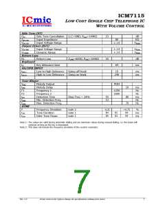
AC CHARACTERISTICS
(ILINE = 15mA, Frequency = 800Hz, unless otherwise specified)
Symbol
Parameter
Test Conditions
Min
Typ
Max
Unit
Transmit (TX)
GTX
THD
ZIN M1,M2
Transmit Gain
Distortion
Input Impedance
LLC=GND, RZAC=100KΩ
VL < 0.5 VRMS
32
33.5
20
35
2
dB
%
KΩ
Differential
Single Ended
VPEAK
VPEAK
± 1.0
± 0.5
VIN M1,M2
Input Voltage Range
Receive (RX)
LLC=GND, RZAC=100KΩ,
Volume=Reset
VRXI < 0.5 VRMS
GRX
Receive Gain
3.5
5.0
6.5
2
dB
THD
ZIN RXI
VIN RXI
Distortion
Input Impedance
Input Voltage Range
%
KΩ
VPEAK
8
± 2.8
Rev. 2.5
ICmic reserves the right to change the specifications without prior notice
6

 ICMIC [ IC MICROSYSTEMS ]