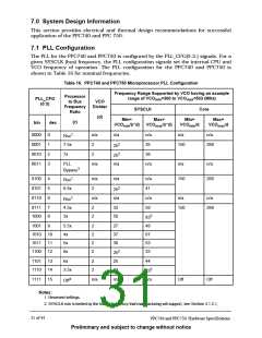
7.0 System Design Information
Th is section provides electrical an d th erm al design recom m en dation s for su ccessfu l
application of th e PPC740 an d PPC 750.
7.1 PLL Configuration
Th e PLL for th e PPC740 an d PPC750 is con figu red by th e PLL_CFG[0-3-] sign als. For a
given SYSCLK (bu s) frequ en cy, th e PLL con figu ration sign als set th e in tern al CPU an d
VCO frequ en cy of operation . Th e PLL con figu ration for th e PPC740 an d PPC750 is
sh own in Table 16 for n om in al frequ en cies.
Table 16. PPC740 and PPC750 Microprocessor PLL Configuration
Frequency Range Supported by VCO having an example
Processor
range of VCO =300 to VCO
=533 (MHz)
PLL_CFG
(0:3)
min
max
to Bus
Frequency
Ratio
VCO
Divider
SYSCLK
Core
(d)
Min=
Max=
VCO /(r*d)
Min=
VCO /d
Max=
VCO /d
max
(r)
bin
dec
VCO /(r*d)
min
max
min
1
0000
0001
0010
0011
0
1
2
3
n/a
2
n/a
n/a
35
n/a
n/a
Rsv
2
7.5x
7x
150
266
25
2
2
38
25
PLL
n/a
n/a
n/a
n/a
n/a
n/a
3
Bypass
1
0100
0101
0110
4
5
6
n/a
2
n/a
41
150
266
Rsv
2
6.5x
25
1
n/a
n/a
n/a
59
n/a
n/a
Rsv
0111
1000
7
8
4.5x
3x
2
2
33
50
150
266
5
83
48
67
53
33
1001
9
5.5x
4x
2
2
2
2
27
37
30
1010 10
1011 11
1100 12
5x
2
8x
25
1101 13
1110 14
6x
2
2
25
43
44
83
5
3.5x
4
1111 15
n/a
n/a
n/a
Off
Off
Off
Notes:
1. Reserved settings.
2. SYSCLK min is limited by the lowest frequency that manufacturing will support, see Section 3.1.2.1,
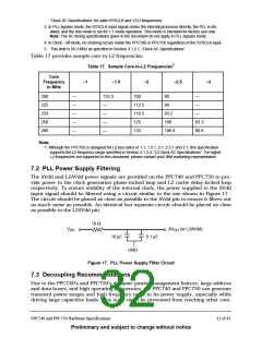
31 of 43
PPC740 and PPC750 Hardware Specifications
Preliminary and subject to change without notice

 IBM [ IBM ]