IBM PowerPC 403GCX
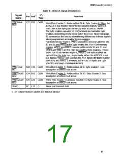
Table 4. 403GCX Signal Descriptions
Signal
Name
I/O
Type
Pin Ball1
Function
DTR/RTS
88 L14
O
Data Terminal Ready / Request to Send. The function of this pin as
either DTR or RTS is selectable via the Serial Port Configuration bit
in the IOCR.
EOT0/TC0
128 A11 I/O
End of Transfer 0 / Terminal Count 0. The function of the EOT0/TC0
is controlled via the EOT/TC bit in the DMA Channel 0 Control Reg-
ister. When EOT0/TC0 is configured as an End of Transfer pin,
external users may stop a DMA transfer by placing a logic 0 on this
input pin. When configured as a Terminal Count pin, the 403GCX
signals the completion of a DMA transfer by placing a logic 0 on this
pin.
EOT1/TC1
EOT2/TC2
131 A10 I/O
132 C10 I/O
End of Transfer 1 / Terminal Count 1. See description of EOT0/TC0.
End of Transfer 2 / Terminal Count 2. See description of EOT0/TC0.
EOT3/TC3/ 133 D10 I/O
XSize0
End of Transfer 3 / Terminal Count 3 / External Master Transfer Size
0. When the 403GCX is bus master, this pin has the same function
as EOT0/TC0.
When the 403GCX is not bus master, EOT3/TC3/XSize0 is used as
one of two external transfer size input bits, XSize0:1.
Error
136 C9
O
System Error. Error goes to a logic 1 whenever a machine check
error is detected in the 403GCX. The Error pin then remains a logic
1 until the machine check error is cleared in the Exception Syn-
drome Register and/or Bus Error Syndrome Register.
1
G7
Ground. All ground pins must be used.
Ground. All ground pins must be used.
Ground. All ground pins must be used.
Ground. All ground pins must be used.
Ground. All ground pins must be used.
Ground. All ground pins must be used.
Ground. All ground pins must be used.
Ground. All ground pins must be used.
Ground. All ground pins must be used.
Ground. All ground pins must be used.
Ground. All ground pins must be used.
10 E2
15 F1
29 J4
30 K1
41 H7
50 N5
59 P7
60 L7
70 P10
81 H8
GND
13

 IBM [ IBM ]