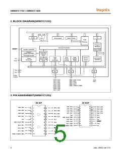
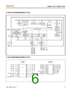
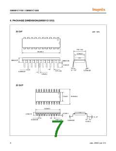
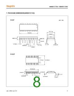
GMS81C1102 / GMS81C1202
8. PIN FUNCTION
VDD: Supply voltage.
VSS: Circuit ground.
RESET: Reset the MCU.
In addition, RA serves the functions of the various special
features in Table 8-1.
RB0~RB4: RB is a 5-bit, CMOS, bidirectional I/O port.
RB pins can be used as outputs or inputs according to “1”
or “0” written in the Port Direction Register(RBIO).
XIN: Input to the inverting oscillator amplifier and input to
the internal clock operating circuit.
RB serves the functions of the various following special
features.
XOUT: Output from the inverting oscillator amplifier. If
RC Option is used, the oscillator frequency divided by 4
(Xin/4) comes out from Xout pin.
Port pin
Alternate function
RA0~RA7: RA is an 8-bit, CMOS, bidirectional I/O port.
RA pins can be used as outputs or inputs according to “1”
or “0” written in the Port Direction Register(RAIO).
RB0
AN0 ( Analog Input Port 0 )
AVref ( External Analog Reference Pin )
BUZ ( Buzzer Driving Output Port )
INT0 ( External Interrupt Input Port 0 )
INT1 ( External Interrupt Input Port 1 )
PWM ( PWM Output )
RB1
RB2
RB3
RB4
Port pin
Alternate function
RA0
RA1
RA2
RA3
RA4
RA5
RA6
RA7
EC0 ( Event Counter Input Source )
AN1 ( Analog Input Port 1 )
AN2 ( Analog Input Port 2 )
AN3 ( Analog Input Port 3 )
AN4 ( Analog Input Port 4 )
AN5 ( Analog Input Port 5 )
AN6 ( Analog Input Port 6 )
AN7 ( Analog Input Port 7 )
COMP0 ( Timer0 Compare Output )
Table 8-2 RB Port
RC0~RC1: RC is a 2-bit, CMOS, bidirectional I/O port.
RC pins can be used as outputs or inputs according to “1”
or “0” written in the Port Direction Register(RCIO)
.
Table 8-1 RA Port
PIN NAME
Pin No.
In/Out
Function
V
V
-
-
I
I
5
14
13
11
12
17
18
19
20
1
Supply voltage
DD
Circuit ground
SS
RESET
Reset signal input
X
IN
X
OUT
O
I/O (Input)
I/O (Input)
I/O (Input)
I/O (Input)
I/O (Input)
I/O (Input)
I/O (Input)
I/O (Input)
I/O (Input)
I/O (Output)
I/O (Input)
I/O (Input)
I/O (Output/Output)
I/O
RA0 (EC0)
RA1 (AN1)
RA2 (AN2)
RA3 (AN3)
RA4 (AN4)
RA5 (AN1)
RA6 (AN1)
RA7 (AN7)
RB0 (AVref/AN0)
RB1 (BUZ)
RB2 (INT0)
RB3 (INT1)
RB4 (PWM/COMP0)
RC0
External Event Counter input
Analog Input Port 1
Analog Input Port 2
Analog Input Port 3
8-bit general I/O ports
Analog Input Port 4
2
Analog Input Port 5
3
Analog Input Port 6
4
Analog Input Port 7
6
Analog Input Port 0 / Analog Reference
Buzzer Driving Output
External Interrupt Input 0
External Interrupt Input 1
PWM Output or Timer Compare Output
7
8
5-bit general I/O ports
2-bit general I/O ports
9
10
15
16
RC1
I/O
Table 8-3 Pin Description
6
Jan. 2002 ver 2.0

 HYNIX [ HYNIX SEMICONDUCTOR ]