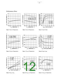
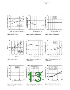
10
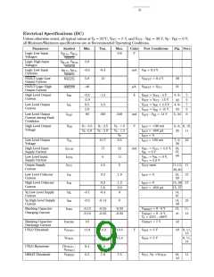
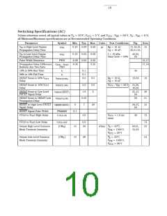
Switching Specifications (AC)
Unless otherwise noted, all typical values at T = 25°C, V
all Minimum/Maximum specifications are at Recommended Operating Conditions.
= 5 V, and V
- V = 30 V, V - V = 0 V;
CC2 EE E EE
A
CC1
Parameter
Symbol
Min.
Typ. Max. Units
Test Conditions
Fig.
Note
VIN to High Level Output
Propagation Delay Time
tPLH
0.10
0.30
0.50
µs
Rg = 10 Ω
Cg = 10 nF,
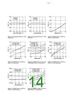
17,18,19, 15
20,21,22,
VIN to Low Level Output
Propagation Delay Time
tPHL
0.10
0.32
0.02
0.50
f = 10 kHz,
45,54,
55
Duty Cycle = 50%
Pulse Width Distortion
PWD
-0.30
-0.35
0.30
0.35
16,17
Propagation Delay Difference (tPHL - tPLH
)
17,18
Between Any Two Parts
10% to 90% Rise Time
90% to 10% Fall Time
PDD
tr
0.1
0.1
0.3
45
tf
DESAT Sense to 90% VOUT
Delay
tDESAT(90%)
0.5
3.0
5
Rg = 10 Ω,
Cg = 10 nF
23,56
19
DESAT Sense to 10% VOUT
Delay
tDESAT(10%)
tDESAT(FAULT)
tDESAT(LOW)
2.0
1.8
0.25
7
V
CC2
- V = 30 V
EE
24,28,
46,56
DESAT Sense to Low Level
FAULT Signal Delay
25,47,
56
20
21
22
DESAT Sense to DESAT Low
Propagation Delay
56
RESET to High Level FAULT tRESET(FAULT)
Signal Delay
3
20
26,27,
56
RESET Signal Pulse Width
PWRESET
tUVLO ON
0.1
UVLO to V
High Delay
4.0
V
= 1.0 ms
49
13
OUT
CC2
ramp
UVLO to V
Low Delay
tUVLO OFF
|CMH|
6.0
30
14
23
OUT
Output High Level Common
Mode Transient Immunity
15
15
kV/µs T = 25°C,
50,51,
52,53
A
V
= 1500 V,
= 30 V
CM
V
CC2
Output Low Level Common
Mode Transient Immunity
|CML|
30
T = 25°C,
24
A
V
CM
= 1500 V,
V
CC2
= 30 V

 HP [ HEWLETT-PACKARD ]