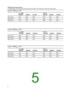
Demo Board Schematic for PA Only
Vdd
C13
C14
14
18
DCS/PCS RFin
Agilent
Vdd
20
C2
C3
DCS/PCS RFout
EGSM RFout
11
C11
C8
21
ACPM-7891
YYWW
Component Component
C9
Label
C2
C3
Value
.033 µF
12 pF
23
24
C4
C5
7
C4
C5
C7
C8
220 pF
.033 µF
220 pF
33 pF
Vdd
26
EGSM RFin
C9
.033 µF
1
4
C11
C13
C14
33 pF
Vdd
.033 µF
27 pF
C7
Pin Description Table
No.
Function
Description
Notes
1
Gnd
2
Vapc EGSM
Gnd
EGSM Control Voltage
EGSM Supply 3rd stage
See datasheet Figure 4
3
4
Vdd3 EGSM
Gnd
3.5V nominal – output stage, bypass with 0.033 µF//220 pF[1]
5
6
Gnd
7
RFout EGSM
Gnd
EGSM Output
50Ω nominal, external d.c. blocking required – 33 pF
8
9
Gnd
10
11
12
13
14
15
16
17
18
19
20
21
22
23
24
25
26
Gnd
RFout DCS/PCS
Gnd
DCS/PCS Output
50Ω nominal, external d.c. blocking required – 33 pF
Gnd
Vdd3 DCS/PCS
Gnd
DCS/PCS Supply 3rd stage
DCS/PCS Control voltage
DCS/PCS Input
3.5V nominal – output stage, bypass with 0.033 µF//27 pF[1]
See datasheet Figure 5 (DCS) and Figure 6 (PCS)
Vapc DCS/PCS
Gnd
RFin DCS/PCS
Gnd
+2 dBm GMSK, 50Ω nominal, internally d.c. blocked
Vdd1,2 DCS/PCS
Vdd1,2 Bypass
Gnd
DCS/PCS Supply 1st and 2nd stages
DCS/PCS 1st and 2nd stage bypassing
3.5V nominal – driver stages, bypass with 0.033 µF
bypass with 12 pF
Vdd1,2 Bypass
Vdd1,2 EGSM
Gnd
EGSM 1st and 2nd stage bypassing
EGSM Supply 1st and 2nd stages
bypass with 220 pF
3.5V nominal – driver stages, bypass with 0.033 µF
RFin EGSM
EGSM Input
+2 dBm GMSK, 50Ω nominal, internally d.c. blocked
Note:
1. In addition a 2.2 µF capacitor should be connected to pins 4 and 14 or alternatively star connections can be made from a single 2.2 µF capacitor keeping
the connection distances as short as possible.
9

 HP [ HEWLETT-PACKARD ]