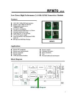
RFM70 V1.0
Table of Contents
1
2
3
4
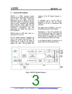
General Description.................................................................................................................
3
4
5
6
Abbreviations ..........................................................................................................................
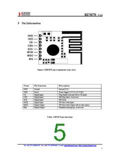
Pin Information .......................................................................................................................
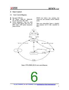
State Control ...........................................................................................................................
4.1 State Control Diagram............................................................................................................... 6
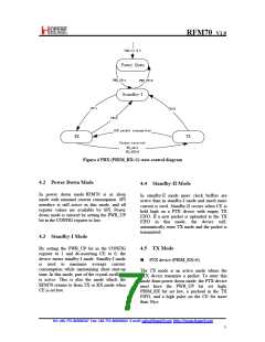
4.2 Power Down Mode.................................................................................................................... 7
4.3 Standby-I Mode......................................................................................................................... 7
4.4 Standby-II Mode........................................................................................................................ 7
4.5 TX Mode ................................................................................................................................... 7
4.6 RX Mode................................................................................................................................... 8
5
Packet Processing .................................................................................................................... 8
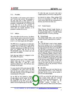
5.1 Packet Format............................................................................................................................ 8
5.1.1 Preamble........................................................................................................................... 9
5.1.2 Address............................................................................................................................. 9
5.1.3 Packet Control.................................................................................................................. 9
5.1.4 Payload........................................................................................................................... 10
5.1.5 CRC................................................................................................................................ 10
5.2 Packet Handling ...................................................................................................................... 10
Data and Control Interface .................................................................................................... 11
6.1 TX/RX FIFO ........................................................................................................................... 11
6.2 Interrupt................................................................................................................................... 11
6.3 SPI Interface............................................................................................................................ 12
6.3.1 SPI Command ................................................................................................................ 12
6.3.2 SPI Timing ..................................................................................................................... 13
Register Map ......................................................................................................................... 15
7.1 Register Bank 0 ....................................................................................................................... 15
7.2 Register Bank 1 ....................................................................................................................... 20
Electrical Specifications ......................................................................................................... 21
Typical Application Schematic............................................................................................... 22
6
7
8
9
10 Package Information.............................................................................................................. 23
11 Order Information................................................................................................................. 25
12 Contact Information .............................................................................................................. 26
Tel: +86‐755‐86096587 Fax: +86‐755‐86096602 E‐mail: sales@hoperf.com http://www.hoperf.com
2

 HOPERF [ HOPERF ]