RF02
GENERAL DEVICE SPECIFICATION
All voltages are referenced to Vss, the potential on the ground reference pin VSS.
Absolute Maximum Ratings (non-operating)
Symbol
Vdd
Parameter
Min
-0.5
-0.5
-0.5
-25
Max
6.0
Units
Positive supply voltage
V
Vin
Voltage on any pin except open collector outputs
Voltage on open collector outputs
Input current into any pin except VDD and VSS
Electrostatic discharge with human body model
Storage temperature
Vdd+0.5
6.0
V
Voc
V
Iin
25
mA
V
ESD
Tst
1000
125
-55
℃
Recommended Operating Range
Symbol
Vdd
Parameter
Min
Max
5.4
Units
V
Positive supply voltage
2.2
Voc
Voltage on open collector outputs (Max 6.0 V)
Ambient operating temperature
Vdd - 1
-40
Vdd + 1
85
V
Top
℃
ELECTRICAL SPECIFICATION
(Min/max values are valid over the whole recommended operating range, typ conditions:
Top =27℃;Vdd =Voc=2.7V)
DC Characteristics
Symbol
Parameter
Conditions/Notes
Min
Typ
Max
Units
Idd_TX_0
Supply current 433 MHz band
Active state with
0dBm
12
14
15
mA
(TX mode,
868 MHz band
915 MHz band
Pout =0dBm)
output power
Idd_TX_PMAX Supply current 433 MHz band
Active state with
maximum output
power
21
23
24
mA
(TX mode,
Pout =Pmax
868 MHz band
915 MHz band
)
Ipd
Iwt
Ilb
Ix
Standby current in sleep mode
(Note 1)
All blocks
disabled
0.3
1.5
0.5
1.5
µA
µA
µA
mA
Wake-up timer current
consumption
Low battery detector current
consumption
Idle current
Only crystal
oscillator is on
Tel: +86-755-82973805
Fax: +86-755-82 E-mail: sales@hoperf.com http://www.hoperf.com

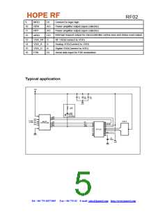
 HOPERF [ HOPERF ]