RF02
up the microcontroller, effectively reducing the period the microcontroller has to be active. The cause of
the interrupt can be read out from the transmitters by the microcontroller through the nIRQ pin.
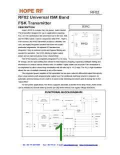
Interface
An SPI compatible serial interface lets the user select the operating frequency band and center
frequency of the synthesizer, polarity and deviation of FSK modulation, and output power level. Division
ratio for the microcontroller clock, wake-up timer period, and low battery detector threshold are also
programmable. Any of these auxiliary functions can be disabled when not needed. All parameters are set
to default after power-on; the programmed values are retained during sleep mode.
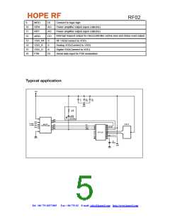
PACKAGE PIN DEFINITIONS
Pin type key: D=digital, A=analog, S=supply, I=input, O=output, IO=input/output
PinP Name
Type Function
1
2
3
4
5
6
7
8
SDI
DI
DI
DI
DO
AIO
S
Data input of serial control interface
SCK
Clock input of serial control interface
Chip select input of serial control interface (active low)
Microcontroller clock (1 MHz-10 MHz)
Crystal connection (other terminal of crystal to VSS)
Digital VSS(Connect to VSS)
nSEL
CLK
XTL
VSS_D
VSS_A
VSS_RF
S
Analog VSS(Connect to VSS)
S
RF VSS(Connect to VSS)
Tel: +86-755-82973805
Fax: +86-755-82 E-mail: sales@hoperf.com http://www.hoperf.com

 HOPERF [ HOPERF ]