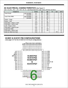
HI-8050/51, HI-8150/51
ABSOLUTE MAXIMUM RATINGS
Voltages referenced to VSS = 0V
Supply Voltage VDD ..........................0V to 7V Operating Temperature Range(Industrial) ....... -40°C to +85°C
VEE................VDD-35V to 0V (Hi-Temp/Mil) ..... -55°C to +125°C
Voltage at any input, except BPIN..-0.3V to VDD+0.3V Storage Temperature .................................... -65°C to +125°C
Voltage at BPIN input ..............VDD-35V to VDD+0.3V
DC current per input pin .....................................10 mA
Power Dissipation............................................500 mW
Solder Temperature (Leads) ..................... +280°C for 10 sec.
(Package) ........................................ +220°C
Junction Temperature, Tj .......................................... £ +175°C
NOTE: Stresses above those listed under "Absolute Maximum Ratings" may cause permanent damage to the device. These a re stress ratings only.
Functional operation of the device at these or any other conditions above those indicated in the operational section s of the specifications is not implied.
Exposure to absolute maximum rating conditions for extended periods may affect device reliability.
VDD = 5V ±5%, VEE = -25V, VSS = 0V, TA = operating temperature range (unless otherwise specified).
PARAMETER
SYMBOL
VDD
IDD
CONDITION
MIN
TYP
MAX
7.0
UNITS
V
Operating Voltage
Supply Current:
3.0
(Converter Off, fBP = 0Hz)
Static, No Load
Static, No Load
Logic Inputs
Logic Inputs
Logic Inputs
Logic Inputs
200
µA
µA
V
IEE
120
0.8
Input Low Voltage, HI-8050/51 only (except BPIN)
Input High Voltage, HI-8050/51 only (except BPIN)
Input Low Voltage, HI-8150/51 only (except BPIN)
Input High Voltage, HI-8150/51 only (except BPIN)
Input Low Voltage, BPIN
VILTTL
VIHTTL
VILCMOS
VIHCMOS
VILX
VIHX
IIN1
0
2
VDD
0.3 VDD
VDD
0.6 VDD
VDD
100
V
0
V
V
V
0.7 VDD
VEE
0.8 VDD
Input High Voltage, BPIN
V
Input Current
Input Current
(except T1 & T2)
(T1 & T2)
VIN = 0V to 5V
VIN = 0V to 5V
nA
µA
pF
KΩ
Ω
mA
mA
V
IIN2
10
Input Capacitance
(Guaranteed, not tested)
CI
RSEG
RBP
10
15
600
-3.0
Segment Output Impedance
Backplane Output Impedance
Da ta Out Current:
IL = 10µA
IL = 10µA @ 25°C
VOH = 4.5
10
450
Source Current
Sink Current
@ No Load
IDOH
IDOL
VEEC
IDD
VEEC
VOS
VOL = 0.4
See Fig. 2
3.2
-22
Voltage Converter:
-21.5
-21
1.8
(VDD - VSS = 5V, TA = 25°C)
@ 0.1mA Load
@ 10KΩ Load
See Fig. 2
See Fig. 2
See Fig. 4
mA
V
mV
-20
Offset Voltage
(Guaranteed, not tested)
25
HOLT INTEGRATED CIRCUITS
5

 HOLTIC [ HOLT INTEGRATED CIRCUITS ]