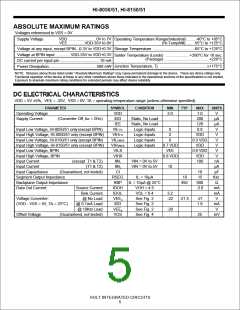
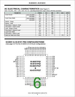
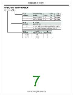
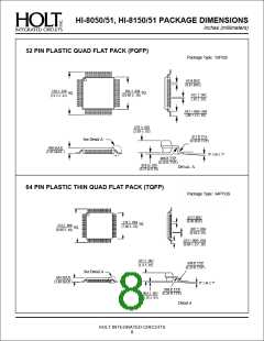
HI-8050/51, HI-8150/51
FUNCTIONAL DESCRIPTION
DOUT
INPUT LOGIC
The DOUT30, DOUT32, and DOUT38 pins are available for
cascading devices to drive more segments (See Figure 3) and
for verifying the integrity of the shift register data. The outputs
can drive 2 TTL loads. They change on the positive edge of
CL .
The data is clocked into a serial shift register from the DIN in-
put on the negative edge of CL while CS is held low. LD is
normally held low and pulsed high only when data from the
shift register is parallel latched to the segment outputs. CS
must be low when LD is pulsed. The latches are transparent
while LD is high. A logic "1" in the shift register causes the
corresponding segment output to be out of phase with the AUTOMATIC SEGMENTS OFF
BP output. All four logic inputs are TTL compatible on the
HI-8050/51and CMOS compatible on the HI-8150/51.
A threshold device detects when the 5V supply is below ap-
proximately 1V and forces all the segments and the backplane
to the same level. This feature is used to discharge the VEE
capacitor when the 5V power is switched off, to prolong the life
of the LCD display.
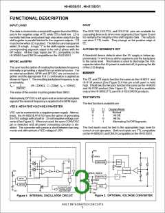
BPOSC and BPIN
The user has the option of creating the backplane frequency
internally or providing a signal from an external source. For
an internal oscillator, BPIN and BPOSC are connected to-
gether and the appropriate R & C combination is applied as
8020OPT
shown in Figure 1. The resulting backplane frequency is ap- The CL and CS inputs function the same as the HI-8010 and
proximately:
HI-8110 product (See Figure 5) if this pin is left open or held
high. If held low, the two pins function the same as the HI-8020
and HI-8120 product (See Figure 6). This input is available
only on the HI-8050 (TTL) and HI-8150 (CMOS) products.
fBP =
1
. (R = 220KW, C = 220pF, fBP ≈ 100HZ)
256 RC
The value of the resistor must be greater than 30KW.
TEST INPUTS
Alternatively, BPOSC is left open and an external backplane
signal of the desired frequency is applied to the BPIN input.
The test functions available are:
VEE & NEGATIVE VOLTAGE CONVERTER
T2
0
0
1
1
T1 Display M ode
0
1
0
1
Normal
All Off
All On
VEE can be connected to a negative power supply. Alterna-
tively, the HI-8050 & HI-8150 have the option of generating
the VEE voltage with a built-in -25 volt negative voltage con-
verter (See Figure 2). When not used, the open CONVOSC
pin is detected and all power consuming circuitry is dis-
abled. The converter will survive a short between two seg-
ments and stillmaintain a VEE voltage of -20V.
Alternating On/Off Segments
The test inputs must be tied to the appropriate logic level for
correct circuit operation. Both test inputs are TTL compatible
on the HI-8050/51 and CMOS compatible on the HI-8150/51.
VDD
68KW
R
C
OSC
CONVOSC
R SENSE
÷ 256
Control
VDD
VDD
Q
IN5818, IN5819
CONVOUT
330µH
R
BPIN
VSS
BPOSC
C
VEE
TO BACKPLANE
TRANSLATOR
AND DRIVER
10µF
VSS
VSS
Figure 2. OPTIONAL VOLTAGE CONVERTER
Figure 1. INTERNAL OSCILLATOR CIRCUIT
HOLT INTEGRATED CIRCUITS
3

 HOLTIC [ HOLT INTEGRATED CIRCUITS ]