Voltages referenced to VSS = 0V
Supply Voltage VDD........................ 0V to 7V
VEE................VDD-35V to 0V
Voltage at any input, except BPIN....-0.3 to VDD+0.3V
Power Dissipation......................................................300 mW
Operating Temperature Range - Industrial...... -40° to +85°C
Operating Temperature Range - Hi-Temp/Mil...-55° to +125°C
Storage Temperature Range............................-65° to +150°C
Voltage at BPIN input.................VDD-35 to VDD+0.3V
DC Current any input pin...................................10 mA
NOTE: Stresses above those listed under "Absolute Maximum Ratings" may cause permanent damage to the device. These a re stress ratings only.
Functional operation of the device at these or any other conditions above those indicated in the operational section s of the specifications is not implied.
Exposure to absolute maximum rating conditions for extended periods may affect device reliability.
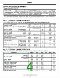
VDD = 5V ±5%, VEE = -21.5V, VSS = 0V, TA = operating temperature range (unless otherwise specified).
PARAMETER
SYMBOL
VDD
IDD
CONDITION
MIN
TYP
MAX
7.0
UNITS
V
Operating Voltage
3.0
Supply Current:
(Converter Off, fBP = 100Hz)
Static, No Load
Static, No Load
300
120
µA
µA
V
V
V
IEE
Input Low Voltage
Input High Voltage
Input Low Voltage
Input High Voltage
Input Current
(excluding BPIN)
(excluding BPIN)
(BPIN)
VIL
VIH
VILX
VIHX
IIN
0
2
0.8
VDD
0.6 VDD
VDD
100
VEE
0.8 VDD
(BPIN)
V
VIN = 0 to 5V
nA
pF
Ω
Input Capacitance
(Guaranteed, not tested)
CI
5
Segment Output Impedance
Backplane Output Impedance
Data Out Current:
RSEG
RBP
IDOH
IDOL
VEEC
IDD
IL = 10µA
IL = 10µA
VOH = 4.5
VOL = 0.4
See Fig. 2
See Fig. 2
See Fig. 2
See Fig. 4
15,000
600
-3.0
Ω
Source Current
Sink Current
@ No Load
@ 0.1mA Load
@ 10KΩ Load
mA
mA
V
mA
V
3.2
-22
Voltage Converter:
(VDD - VSS = 5V, TA = 25°C)
-21.5
-21
1.8
VEEC
VOS
-20
Offset Voltage
(Guaranteed, not tested)
25
mV
VDD = 5V , VEE = -21.5V, VSS = 0V, TA = operating temperature range (unless otherwise specified).
PARAMETER
SYMBOL
tCL
VDD
5V
5V
5V
5V
5V
5V
5V
MIN
250
500
125
250
80
TYP
MAX
UNITS
ns
Clock Period
non-cascaded
cascaded
tCL
ns
Clock Pulse Width
non-cascaded
cascaded
tCW
tCW
tDS
ns
ns
Data In - Setup
ns
Data In - Hold
tDH
80
ns
Chip Select - Setup to Clock
tCSS
100
ns
Chip Select - Hold to Clock
Load - Setup to Clock
tCSH
tLS
5V
5V
120
120
ns
ns
Chip Select - Setup to Load
Load Pulse Width
Chip Select - Hold to Load
Data Out Valid, from Clock
tCSL
tLW
tLCS
tCDO
5V
5V
5V
5V
0
ns
ns
ns
ns
130
120
170
HOLT INTEGRATED CIRCUITS
3-18

 HOLTIC [ HOLT INTEGRATED CIRCUITS ]