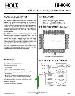
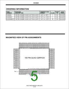
HI-8040
FUNCTIONAL DESCRIPTION
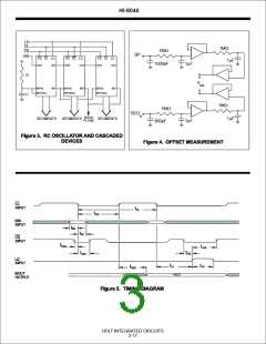
DOUT
INPUT LOGIC
The DOUT pin is available from segment 85 for cascading
devices to drive more segments and for verifying the data
integrity. This output can drive 2 TTL loads. It changes on the
positive edge of CL .
CS must be held low to enter data into the shift register.
The data is clocked on the negative edge of CL . LD is nor-
mally held low and only pulsed high when new data is ready
for display. When LD is high the latch is transparent. All four
logic inputs are TTL compatible. A logic "1" at DIN that is
eventually latched to the segment drivers will cause the seg-
ment to be at the opposite voltage level of the BP pin (out of
phase).
AUTOMATIC SEGMENTS OFF
The internal backplane signal is tested continuously to be at
least 10Hz. If the detector senses f<10Hz, then the segments
are forced to the same voltage as the backplane (all segments
in "OFF" state). However, the detector is only functional while
VDD is above the minimum operating voltage specification.
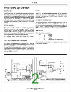
BPOSC and BPIN
The user can either make an oscillator to create the
backplane frequency or drive a signal into BPIN leaving
BPOSC open. To make an oscillator, pins BPOSC and
BPIN must be connected togeth er and the appropriate R
and C combination applied (See Figure 1). If the oscillator is
used, the backplane frequency is approximately
1
TEST INPUTS
The test functions available are:
T2
0
T1
0
Display
Normal
fBP =
.
(for R = 180KΩ & C = 220pF, fBP ≈ 100Hz).
0
1
All Off
256 RC
1
0
All On
1
1
Alternating On/Off Segments
VEE & NEGATIVE VOLTAGE CONVERTER
Th e test inputs must be tied to the appropriate logic level for
correct circuit operation.
VEE may be externally driven to a maximum -30V. Alterna-
tively, there is a voltage converter that will provide -21.4 volts
(See Figure 2). If the converter pins are left open circuit, an
on-chip sense resistor will cause shut down of all current
consumption associated with the converter. The converter
will survive a shorted segment condition and continue to
maintain VEE at -20 volts.
VDD
R 330KΩ
OSC
R SENSE
Control
IN5818, IN5819
VDD
330µh
VSS
10µF
VSS
HOLT INTEGRATED CIRCUITS
3-16

 HOLTIC [ HOLT INTEGRATED CIRCUITS ]