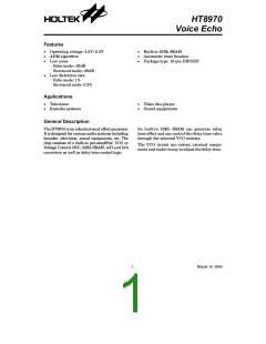
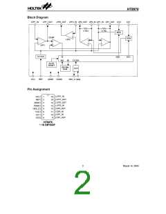
HT8970
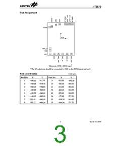
Pad Description
Internal
Connection
Pad No.
Pad Name
I/O
Description
1
2
DGND
OSC_O
I
Digital ground
System oscillator output
¾
¾
O
System oscillator input, system frequency
adjustable pin
3
VCO
I
¾
4
5
CC1
Current control 1
Current control 0
OP1 output
¾
¾
O
I
¾
¾
¾
¾
¾
¾
¾
¾
¾
¾
¾
¾
¾
CC0
6
OP1_OUT
OP1_IN
OP2_IN
OP2_OUT
LPF2_IN
LPF2_OUT
LPF1_OUT
LPF1_IN
VCC
7
OP1 input
8
I
OP2 input
9
O
I
OP2 output
10
11
12
13
14
15
16
Low pass filter 2 input
Low pass filter 2 output
Low pass filter 1 output
Low pass filter 1 input
Analog and positive power supply
Analog reference voltage
Analog ground
O
O
I
I
REF
I
AGND
I
Absolute Maximum Ratings
Supply Voltage.................................-0.3V to 6V
Input Voltage.................VSS-0.3V to VDD+0.3V
Storage Temperature.................-50°C to 125°C
Operating Temperature ..............-20°C to 70°C
Note: These are stress ratings only. Stresses exceeding the range specified under ²Absolute Maxi-
mum Ratings² may cause substantial damage to the device. Functional operation of this device
at other conditions beyond those listed in the specification is not implied and prolonged expo-
sure to extreme conditions may affect device reliability.
4
March 14, 2000

 HOLTEK [ HOLTEK SEMICONDUCTOR INC ]