HT46R01B/02B/01N/02N
HT48R01B/02B/01N/02N
·
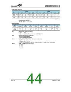
ACSR Register
Bit
Name
R/W
7
TEST
R/W
1
6
ADONB
R/W
0
5
4
3
2
ADCS2
R/W
0
1
ADCS1
R/W
0
0
ADCS0
R/W
0
¾
¾
¾
¾
¾
¾
¾
¾
¾
POR
Bit 7
Bit 6
TEST: for test mode use only
ADONB: ADC module power on/off control bit
0: ADC module power on
1: ADC module power off
Note: 1. it is recommended to set ADONB=1 before entering sleep for saving power.
2. ADONB=1 will power down the ADC module.
Bit 5~3
Bit 2~0
unimplemented, read as ²0²
ADCS2~ADCS0 : Select A/D converter clock source
000: system clock/2
001: system clock/8
010: system clock/32
011: undefined, can¢t be used.
100: system clock
101: system clock/4
110: system clock/16
111: undefined, can¢t be used.
The ADCR control register also contains the
PCR3~PCR0 bits which determine which pins on
PA0~PA3 are used as analog inputs for the A/D converter
and which pins are to be used as normal I/O pins. Note
that if the PCR3~PCR0 bits are all set to zero, then all the
PA0~PA3 pins will be setup as normal I/Os.
The A/D converter overall on/off control is a function of
both the ADONB bit in the ACSR register and the PCRn
bits in the ADCR register as shown in the table. Either
the ADONB bit cleared to zero or the PCRn bits set to a
zero value will switch off the A/D converter. These are
important consideration in power sensitive applications
and must be taken into account if power consumption is
to be minimised. As the table illustrates, execution of the
HALT instruction has no effect on the A/D converter
on/off control and subsequently its power consumption.
The START bit in the register is used to start and reset
the A/D converter. When themicrocontroller sets this bit
from low to high and then low again, an analog to digital
conversion cycle will be initiated. When the START bit is
brought from low to high but not low again, the EOCB bit
in the ADCR register will be set to a ²1² and the analog
to digital converter will be reset. It is the START bit that is
used to control the overall start operation of the internal
analog to digital converter.
PCRn
Bits
HALT
ADONB
Bit
ADC
Instruction
On/Off
= 0
> 0
> 0
X
X
X
X
0
1
Off
On
Off
The EOCB bit in the ADCR register is used to indicate
when the analog to digital conversion process is com-
plete. This bit will be automatically set to ²0² by the
microcontroller after a conversion cycle has ended. In
addition, the corresponding A/D interrupt request flag
will be set in the interrupt control register, and if the inter-
rupts are enabled, an appropriate internal interrupt sig-
nal will be generated. This A/D internal interrupt signal
will direct the program flow to the associated A/D inter-
nal interrupt address for processing. If the A/D internal
interrupt is disabled, the microcontroller can be used to
poll the EOCB bit in the ADCR register to check whether
it has been cleared as an alternative method of detect-
ing the end of an A/D conversion cycle.
Note: X: Don¢t care
A/D Converter On/Off Control
Although the A/D clock source is determined by the sys-
tem clock fSYS, and by bits ADCS2, ADCS1 and ADCS0,
there are some limitations on the maximum A/D clock
source speed that can be selected. As the minimum value
of permissible A/D clock period, tAD, is 0.5ms, care must be
taken for system clock speeds equal to or greater than
4MHz. For example, the system clock operates at a fre-
quency of 4MHz, the ADCS2, ADCS1 and ADCS0 bits
should not be set to ²100². Doing so will give A/D clock pe-
riods that are less than the minimum A/D clock period
which may result in inaccurate A/D conversion values. Re-
fer to the following table for examples, where values
marked with an asterisk * show where, depending upon
the device, special care must be taken, as the values may
be less than the specified minimum A/D Clock Period.
The clock source for the A/D converter, which originates
from the system clock fSYS, is first divided by a division
ratio, the value of which is determined by the ADCS2,
ADCS1 and ADCS0 bits in the ACSR register.
Rev.1.10
45
February 12, 2010

 HOLTEK [ HOLTEK SEMICONDUCTOR INC ]