HT46R23/HT46C23
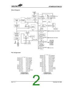
Pad Description
Pad Name
I/O
Option
Description
PA0~PA2
PA3/PFD
PA4/TMR
PA5/INT
Bidirectional 8-bit input/output port. Each bit can be configured as wake-up
input by options. Software instructions determine the CMOS output or
Schmitt trigger input with or without pull-high resistor (determined by
pull-high options: bit option). The PFD, TMR and INT are pin-shared with
Pull-high
Wake-up
I/O
PA3 or PFD
PA6/SDA
PA7/SCL
I/O or Serial Bus PA3, PA4 and PA5, respectively. Once the I2C Bus function is used, the in-
ternal registers related to PA6 and PA7 can not be used.
PB0/AN0
PB1/AN1
PB2/AN2
PB3/AN3
PB4/AN4
PB5/AN5
PB6/AN6
PB7/AN7
Bidirectional 8-bit input/output port. Software instructions determine the
CMOS output, Schmitt trigger input with or without pull-high resistor (deter-
I/O
Pull-high
Pull-high
mined by pull-high: port option) or A/D input.
Once a PB line is selected as an A/D input (by using software control), the
I/O function and pull-high resistor are disabled automatically.
Bidirectional 5-bit input/output port. Software instructions determine the
CMOS output, Schmitt trigger input with or without pull-high resistor (deter-
mine by pull-high option: port option).
PC0~PC4
I/O
I/O
Bidirectional 2-bit input/output port. Software instructions determine the
CMOS output, Schmitt trigger input with or without a pull-high resistor (de-
termined by pull-high option: port option). The PWM0/PWM1 output func-
tion are pin-shared with PD0/PD1 (dependent on PWM options).
PD0/PWM0
PD1/PWM1
Pull-high
I/O or PWM
RES
VDD
VSS
I
Schmitt trigger reset input. Active low.
Positive power supply
¾
¾
¾
¾
¾
Negative power supply, ground.
OSC1, OSC2 are connected to an RC network or a Crystal (determined by
options) for the internal system clock. In the case of RC operation, OSC2 is
the output terminal for 1/4 system clock.
OSC1
OSC2
I
Crystal
or RC
O
TEST1
TEST2
TEST3
TEST mode input pin.
I
¾
It disconnects in normal operation.
Absolute Maximum Ratings
Supply Voltage...........................VSS-0.3V to VSS+6.0V
Input Voltage..............................VSS-0.3V to VDD+0.3V
Storage Temperature............................-50°C to 125°C
Operating Temperature...........................-40°C to 85°C
Note: These are stress ratings only. Stresses exceeding the range specified under ²Absolute Maximum Ratings² may
cause substantial damage to the device. Functional operation of this device at other conditions beyond those
listed in the specification is not implied and prolonged exposure to extreme conditions may affect device reliabil-
ity.
Rev. 2.11
3
December 29, 2008
图片预览")
 HOLTEK [ HOLTEK SEMICONDUCTOR INC ]