HT46R064B/065B/066B
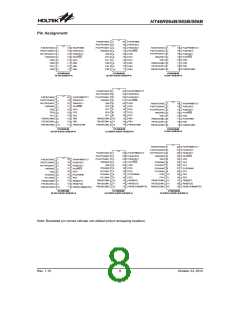
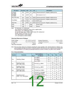
Pin Name
PC0/AN4
Function OPT
I/T
O/T
Description
PCn
ANn
PCPU ST CMOS General purpose I/O. Register enabled pull-up.
PC1/AN5
PC6/AN6
PC7/AN7
ADCR AN A/D channel 4, 5, 6, 7
¾
PC2, PC4~PC5
PCn
PCn
PCPU ST CMOS General purpose I/O. Register enabled pull-up.
PCPU ST CMOS General purpose I/O. Register enabled pull-up.
PC3/PWM1
PWM1 CTRL0
CMOS PWM output
¾
PD0~PD3
VDD
PDn
VDD
VSS
PDPU ST CMOS General purpose I/O. Register enabled pull-up.
PWR
PWR
Power supply
Ground
¾
¾
¾
¾
VSS
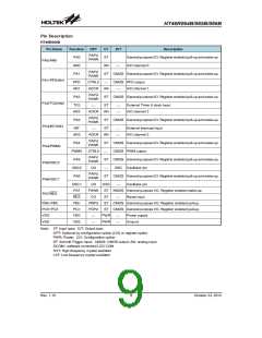
Note: I/T: Input type; O/T: Output type
OPT: Optional by configuration option (CO) or register option
PWR: Power; CO: Configuration option
ST: Schmitt Trigger input; CMOS: CMOS output; AN: analog input
SCOM: Software controlled LCD COM
HXT: High frequency crystal oscillator
LXT: Low frequency crystal oscillator
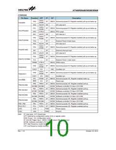
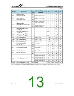
Absolute Maximum Ratings
Supply Voltage...........................VSS-0.3V to VSS+6.0V
Input Voltage..............................VSS-0.3V to VDD+0.3V
Storage Temperature............................-50°C to 125°C
Operating Temperature...........................-40°C to 85°C
I
OL Total ..............................................................100mA
I
OH Total............................................................-100mA
Total Power Dissipation .....................................500mW
Note: These are stress ratings only. Stresses exceeding the range specified under ²Absolute Maximum Ratings² may
cause substantial damage to the device. Functional operation of this device at other conditions beyond those listed
in the specification is not implied and prolonged exposure to extreme conditions may affect device reliability.
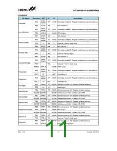
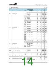
D.C. Characteristics
Ta=25°C
Test Conditions
Conditions
Symbol
Parameter
Min.
Typ.
Max.
Unit
VDD
fSYS=4MHz
2.2
3.0
4.5
¾
5.5
5.5
5.5
1.2
2.25
2.1
4.2
V
¾
¾
VDD
fSYS=8MHz
Operating Voltage
V
¾
fSYS=12MHz
V
¾
3V
5V
3V
5V
0.8
1.5
1.4
2.8
mA
mA
mA
mA
Operating Current
(HXT, HIRC, ERC)
IDD1
No load, fSYS=4MHz
¾
¾
Operating Current
(HXT, HIRC, ERC)
IDD2
No load, fSYS=8MHz
No load, fSYS=12MHz
¾
Operating Current
(HXT, HIRC, ERC)
IDD3
5V
4
6
mA
¾
No load, fSYS=32768Hz
(LXT on OSC1/OSC2,
LVR disabled, LXTLP=1)
5
12
5
10
24
10
20
3V
5V
3V
5V
¾
¾
¾
¾
mA
mA
mA
mA
Operating Current
IDD4
(HIRC + LXT, Slow Mode)
No load, fSYS=32768Hz
(LXT on XT1/XT2,
10
LVR disabled, LXTLP=1)
Rev. 1.10
12
October 23, 2012

 HOLTEK [ HOLTEK SEMICONDUCTOR INC ]