HT45R37
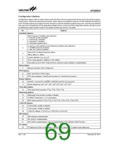
Configuration Options
Configuration options refer to certain options within the MCU that are programmed into the device during the program-
ming process. During the development process, these options are selected using the HT-IDE software development
tools. As these options are programmed into the device using the hardware programming tools, once they are selected
they cannot be changed later as the application software has no control over the configuration options. All options must
be defined for proper system function, the details of which are shown in the table.
No.
Options
Oscillator Options
High Frequency Oscillator type selection
1. External Crystal Oscillator
2. External RC Oscillator
3. Internal RC Oscillator
4. Externally supplied clock
1
fSL and fSUB clock selection (Low frequency oscillator type selection)
1. 32768Hz External Oscillator
2
3
2. 32K_INT Internal Oscillator
Internal RC Oscillator frequency select:
4MHz, 8MHz or 12MHz
4
5
6
fS clock selection: fSUB or fSYS/4
XTAL mode selection: 455kHz or 1M~12MHz
Fast wake-up from HALT mode (Only for external crystal oscillator): enable/disable
Reset Option
7
Rest pin Function: PC0 or Reset Pin
PFD Options
8
9
PA3: normal I/O or PFD output
PFD clock selection: Timer/Event Counter 0 or Timer/Event Counter 1
Buzzer Options
10
11
PA0/PA1: normal I/O or BZ/BZ or PA0=BZ and PA1 as normal I/O
Buzzer frequency: fS/22, fS/23, fS/24, fS/25, fS/26, fS/27, fS/28, fS/29
Time Base Option
12
Time base time-out period: 212/fS, 213/fS, 214/fS, 215/fS
Watchdog Options
13
14
15
Watchdog Timer function: enable or disable
CLRWDT instructions: 1 or 2 instructions
WDT time-out period: 212/fS~213/fS, 213/fS~214/fS, 214/fS~215/fS, 215/fS~216/fS
LVD/LVR Options
16
17
18
LVD function: enable or disable
LVR function: enable or disable
LVR/LVD voltage: 2.1V/2.2V or 3.15V/3.3V or 4.2V/4.4V
SPI Options
19
SIM interface enable/disable
20
SPI_WCOL: enable/disable
21
SPI_CSEN: enable/disable, used to enable/disable (1/0) software CSEN function
I2C Option
22
I2C debounce Time: no debounce, 1 system clock debounce, 2 system clock debounce
Rev. 1.20
69
February 25, 2011
图片预览")
 HOLTEK [ HOLTEK SEMICONDUCTOR INC ]