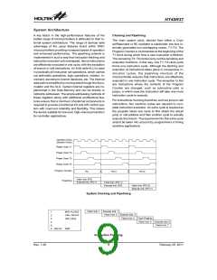
HT45R37
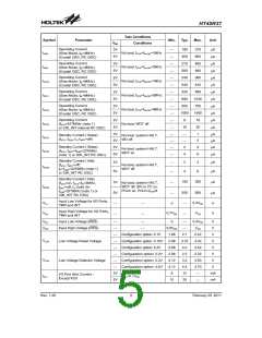
Configuration
Option
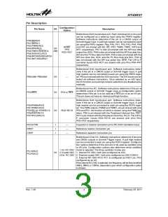
Pin Name
I/O
Description
Bidirectional 2-line I/O. Software instructions determine if the pins
are CMOS outputs or Schmitt Trigger inputs. A pull high resistor
can be connected to each pin using the PCPU register. Configura-
tion options determine if the pins are to be used as oscillator pins
or I/O pins. If configuration options select oscillator pins, the pins
are connected to a 32768Hz crystal oscillator.
PC3/OSC3
I/O
RTC OSC
PC4/OSC4
VDD/AVDD
VSS/AVSS
Positive power supply/analog positive power supply.
¾
¾
¾
¾
Negative power supply, ground/analog negative power supply,
ground
Note: The Pin Description table represents the largest package available, therefore some of the pins and functions
may not be available on smaller package types.
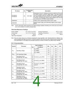
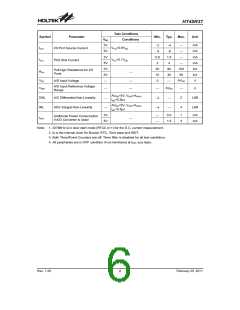
Absolute Maximum Ratings
Supply Voltage...........................VSS-0.3V to VSS+6.0V
Input Voltage..............................VSS-0.3V to VDD+0.3V
Storage Temperature............................-50°C to 125°C
Operating Temperature...........................-40°C to 85°C
I
OL Total ................................................................80mA
I
OH Total..............................................................-80mA
Total Power Dissipation .....................................500mW
Note: These are stress ratings only. Stresses exceeding the range specified under ²Absolute Maximum Ratings² may
cause substantial damage to the device. Functional operation of this device at other conditions beyond those listed
in the specification is not implied and prolonged exposure to extreme conditions may affect device reliability.
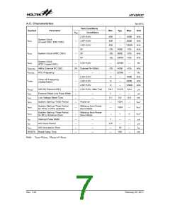
D.C. Characteristics
Ta=25°C
Test Conditions
Conditions
Symbol
Parameter
Min.
Typ.
Max.
Unit
VDD
f
SYS=4MHz
2.2
3.0
4.5
2.7
¾
5.5
5.5
V
¾
VDD
fSYS=8MHz
Operating Voltage
V
¾
¾
fSYS=12MHz
5.5
V
¾
AVDD
A/D Operating Voltage
5.5
V
¾
3V
5V
3V
5V
3V
5V
3V
5V
¾
¾
170
380
240
490
440
900
380
720
250
700
360
800
660
1350
570
1080
mA
mA
mA
mA
mA
mA
mA
mA
Operating Current
IDD1
No load, fSYS=fM=1MHz
No load, fSYS=fM=2MHz
(Crystal OSC, RC OSC)
¾
¾
Operating Current
IDD2
IDD3
IDD4
(Crystal OSC, RC OSC)
¾
¾
Operating Current
No load, fSYS=fM=4MHz
(note 4)
(Crystal OSC, RC OSC)
¾
¾
Operating Current
No load, fSYS=fM=4MHz
(EC Mode, Filter On)
¾
Operating Current
IDD5
No load, fSYS=fM=8MHz
No load, fSYS=fM=12MHz
5V
5V
1.8
2.6
2.7
4.0
mA
mA
¾
¾
(Crystal OSC, RC OSC)
Operating Current
IDD6
(Crystal OSC, RC OSC)
Operating Current
150
340
220
510
3V
5V
¾
¾
mA
mA
IDD7
No load, fSYS=fSLOW=500kHz
(Slow Mode, fM=4MHz)
(Crystal OSC, RC OSC)
Rev. 1.20
4
February 25, 2011
图片预览")
 HOLTEK [ HOLTEK SEMICONDUCTOR INC ]