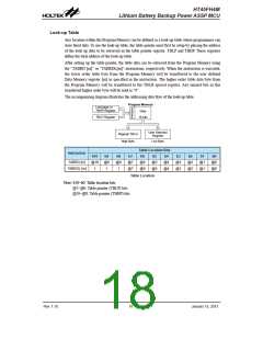
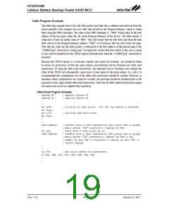
HT45FH4M
Lithium Battery Backup Power ASSP MCU
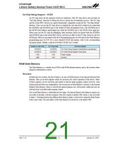
On-Chip Debug Support – OCDS
AnꢀEVꢀchipꢀexistsꢀforꢀtheꢀpurposesꢀofꢀdeviceꢀemulation.ꢀThisꢀEVꢀchipꢀdeviceꢀalsoꢀprovidesꢀanꢀ
“On-ChipꢀDebug”ꢀfunctionꢀtoꢀdebugꢀtheꢀdeviceꢀduringꢀtheꢀdevelopmentꢀprocess.ꢀTheꢀEVꢀchipꢀ
andꢀtheꢀactualꢀMCUꢀdevicesꢀareꢀalmostꢀfunctionallyꢀcompatibleꢀexceptꢀforꢀtheꢀ“On-ChipꢀDebug”ꢀ
function.ꢀUsersꢀcanꢀuseꢀtheꢀEVꢀchipꢀdeviceꢀtoꢀemulateꢀtheꢀrealꢀchipꢀdeviceꢀbehaviorꢀbyꢀconnectingꢀ
theꢀOCDSDAꢀandꢀOCDSCKꢀpinsꢀtoꢀtheꢀHoltekꢀHT-IDEꢀdevelopmentꢀtools.ꢀTheꢀOCDSDAꢀpinꢀisꢀ
theꢀOCDSꢀData/Addressꢀinput/outputꢀpinꢀwhileꢀtheꢀOCDSCKꢀpinꢀisꢀtheꢀOCDSꢀclockꢀinputꢀpin.ꢀ
WhenꢀusersꢀuseꢀtheꢀEVꢀchipꢀforꢀdebugging,ꢀotherꢀfunctionsꢀwhichꢀareꢀsharedꢀwithꢀtheꢀOCDSDAꢀ
andꢀOCDSCKꢀpinsꢀinꢀtheꢀactualꢀMCUꢀdeviceꢀwillꢀhaveꢀnoꢀeffectꢀinꢀtheꢀEVꢀchip.ꢀHowever,ꢀtheꢀtwoꢀ
OCDSꢀpinsꢀwhichꢀareꢀpin-sharedꢀwithꢀtheꢀICPꢀprogrammingꢀpinsꢀareꢀstillꢀusedꢀasꢀtheꢀFlashꢀMemoryꢀ
programmingꢀpinsꢀforꢀICP.ꢀForꢀaꢀmoreꢀdetailedꢀOCDSꢀdescription,ꢀreferꢀtoꢀtheꢀcorrespondingꢀ
documentꢀnamedꢀ“Holtekꢀe-Linkꢀforꢀ8-bitꢀMCUꢀOCDSꢀUser’sꢀGuide”.
Holtek e-Link Pins
OCDSDA
OCDSCK
VDD
EV Chip Pins
OCDSDA
OCDSCK
VDD
Pin Description
On-Chip Debꢀg Sꢀppoꢁt Data/Addꢁess inpꢀt/oꢀtpꢀt
On-Chip Debꢀg Sꢀppoꢁt Clock inpꢀt
Poweꢁ Sꢀpplꢂ
GND
VSS
Gꢁoꢀnd
RAM Data Memory
TheꢀDataꢀMemoryꢀisꢀaꢀvolatileꢀareaꢀofꢀ8-bitꢀwideꢀRAMꢀinternalꢀmemoryꢀandꢀisꢀtheꢀlocationꢀwhereꢀ
temporaryꢀinformationꢀisꢀstored.
Structure
Dividedꢀintoꢀtwoꢀsections,ꢀtheꢀfirstꢀofꢀtheseꢀisꢀanꢀareaꢀofꢀRAM,ꢀknownꢀasꢀtheꢀSpecialꢀFunctionꢀDataꢀ
Memory.ꢀHereꢀareꢀlocatedꢀregistersꢀwhichꢀareꢀnecessaryꢀforꢀcorrectꢀoperationꢀofꢀtheꢀdevice.ꢀManyꢀ
ofꢀtheseꢀregistersꢀcanꢀbeꢀreadꢀfromꢀandꢀwrittenꢀtoꢀdirectlyꢀunderꢀprogramꢀcontrol,ꢀhowever,ꢀsomeꢀ
remainꢀprotectedꢀfromꢀuserꢀmanipulation.ꢀTheꢀsecondꢀareaꢀofꢀDataꢀMemoryꢀisꢀknownꢀasꢀtheꢀGeneralꢀ
PurposeꢀDataꢀMemory,ꢀwhichꢀisꢀreservedꢀforꢀgeneralꢀpurposeꢀuse.ꢀAllꢀlocationsꢀwithinꢀthisꢀareaꢀareꢀ
readꢀandꢀwriteꢀaccessibleꢀunderꢀprogramꢀcontrol.
TheꢀoverallꢀDataꢀMemoryꢀisꢀsubdividedꢀintoꢀtwoꢀbanks.ꢀTheꢀSpecialꢀPurposeꢀDataꢀMemoryꢀregistersꢀareꢀ
accessibleꢀinꢀallꢀbanks,ꢀwithꢀtheꢀexceptionꢀofꢀtheꢀEECꢀregisterꢀatꢀaddressꢀ40H,ꢀwhichꢀisꢀonlyꢀaccessibleꢀ
inꢀBankꢀ1.ꢀSwitchingꢀbetweenꢀtheꢀdifferentꢀDataꢀMemoryꢀbanksꢀisꢀachievedꢀbyꢀsettingꢀtheꢀBankꢀPointerꢀ
toꢀtheꢀcorrectꢀvalue.ꢀTheꢀstartꢀaddressꢀofꢀtheꢀDataꢀMemoryꢀforꢀtheꢀdeviceꢀisꢀtheꢀaddressꢀ00H.
Rev. 1.10
ꢅ1
�anꢀaꢁꢂ 1ꢃꢄ ꢅ01ꢆ

 HOLTEK [ HOLTEK SEMICONDUCTOR INC ]