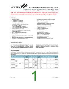
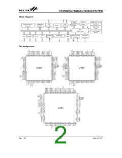
HT37B90/HT37B70/HT37B50/HT37B30
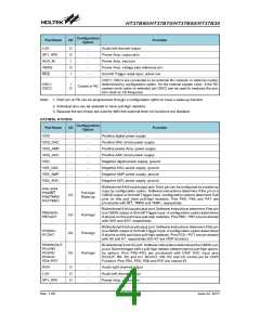
Pad Description
HT37B90, HT37B70
Configuration
Option
Pad Name
VDD
I/O
Function
Positive digital power supply
¾
¾
¾
¾
¾
¾
¾
¾
¾
¾
¾
¾
¾
¾
¾
¾
VDD_DAC
VDD_AMP
VDD_ADC
VSS
Positive DAC circuit power supply
Positive power Amp. power supply
Positive ADC circuit power supply
Negative digital power supply, ground
Negative DAC power supply, ground
Negative AMP power supply, ground
Negative ADC power supply, ground
VSS_DAC
VSS_AMP
VSS_ADC
Bidirectional 8-bit input/output port. Each pin can be configured as a wake-up
input by configuration option. Software instructions determine if the pin is a
CMOS output or Schmitt Trigger input. Configuration options determine if all
pins on this port have pull-high resistors. Pins PA5, PA6 and PA7 are
pin-shared with INT, TMR0 and TMR1, respectively.
PA0~PA4
PA5/INT
Wake-up,
Pull-high
or None
I/O
PA6/TMR0
PA7/TMR1
Bidirectional 8-bit input/output port. Software instructions determine if the pin
is a CMOS output or Schmitt Trigger input. A configuration option determines
if all pins on this port have pull-high resistors. Pins PB0 ~ PB7 are pin-shared
with AD0 and AD7, respectively.
PB0/AD0~
PB7/AD7
Pull-high
or None
I/O
I/O
Bidirectional 8-bit input/output port. Software instructions determine if the pin
is a CMOS output or Schmitt Trigger input. A configuration option determines
if all pins on this port have pull-high resistors. Pins PC0 ~ PC7 are pin-shared
with K0 and K7, respectively (K0~K7 are CR/F function).
PC0/K0~
PC7/K7
Pull-high
or None
Bidirectional 8-bit input/output port. Software instructions determine if the pin
is a CMOS output or Schmitt Trigger input. A configuration option determines
if all pins on this port have pull-high resistors. Pins PD0~PD3 are pin-shared
with R/F OSC input pins RCOUT, RR, RC and CC. PD4~PD6 are pin-shared
with IIS interface pins WAS, DT and CK. PD7 is normal I/O port.
RCOUT: Capacitor or resistor connection pin to RC OSC
RR: Oscillation input pin
PD0/RCOUT
PD1/RR
PD2/RC
PD3/CC
PD4/WAS
PD5/DT
PD6/CK
PD7
Pull-high
or None
I/O
RC: Reference resistor connection pin
CC: Reference capacitor connection pin
WAS, DT and CK control pin for IIS function
WAS: IIS word select output
DT: IIS data transmit output
CK: IIS serial clock output
Bidirectional 8-bit input/output port. Software instructions determine if the pin
is a CMOS output or Schmitt Trigger input. A configuration option determines
if all pins on this port have pull-high resistors. Pins PE0~PE2 are pin-shared
with UART interface pins Min, Mout and Mth. Pins PE3~PE6 are pin-shared
with SPI interface pins SDO, SDI, SCS and SCK. PE7 is normal I/O port.
Min, Mout and Mth control pin for UART Function
Min: MIDI input
PE0/Min
PE1/Mout
PE2/Mth
PE3/SDO
PE4/SDI
PE5/SCS
PE6/SCK
PE7
Pull-high
or None
I/O
Mout: MIDI output
Mth: MIDI through
SDO, SDI, SCS and SCK control pin for SPI Function
SDO: SPI data output pin
SDI: SPI data input pin
SCS: SPI slave select signal.
SCK: SPI clock
RCH
O
Audio right channel output
¾
Rev. 1.00
3
June 22, 2017

 HOLTEK [ HOLTEK SEMICONDUCTOR INC ]